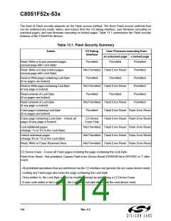
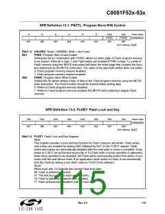
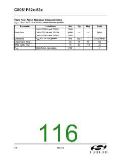
C8051F52x-53x
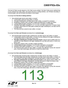
14. Port Input/Output
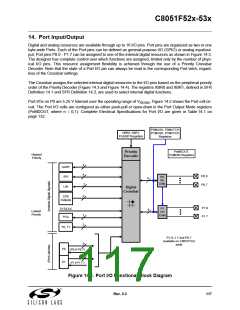
Digital and analog resources are available through up to 16 I/O pins. Port pins are organized as two or one
byte-wide Ports. Each of the Port pins can be defined as general-purpose I/O (GPIO) or analog input/out-
put; Port pins P0.0 - P1.7 can be assigned to one of the internal digital resources as shown in Figure 14.3.
The designer has complete control over which functions are assigned, limited only by the number of phys-
ical I/O pins. This resource assignment flexibility is achieved through the use of a Priority Crossbar
Decoder. Note that the state of a Port I/O pin can always be read in the corresponding Port latch, regard-
less of the Crossbar settings.
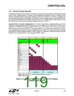
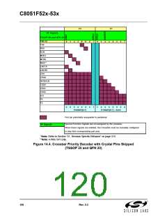
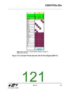
The Crossbar assigns the selected internal digital resources to the I/O pins based on the peripheral priority
order of the Priority Decoder (Figure 14.3 and Figure 14.4). The registers XBR0 and XBR1, defined in SFR
Definition 14.1 and SFR Definition 14.2, are used to select internal digital functions.
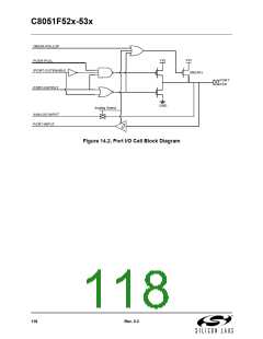
Port I/Os on P0 are 5.25 V tolerant over the operating range of V
. Figure 14.2 shows the Port cell cir-
REGIN
cuit. The Port I/O cells are configured as either push-pull or open-drain in the Port Output Mode registers
(PnMDOUT, where n = 0,1). Complete Electrical Specifications for Port I/O are given in Table 14.1 on
page 132.
P0MASK, P0MATCH
P1MASK, P1MATCH
Registers
XBR0, XBR1,
PnSKIP Registers
PnMDOUT,
PnMDIN Registers
Priority
Decoder
Highest
Priority
2
4
UART
SPI
P0.0
P0.7
P0
I/O
Cells
8
2
LIN
Digital
Crossbar
2
CP0
Outputs
P1.0
P1.7
P1
I/O
Cells
SYSCLK
PCA
8
Lowest
Priority
7
2
T0, T1
P1.0–1.7 and P0.7
available on C8051F53x
parts
8
P0
P1
(P0.0-P0.7)
8
(P1.0-P1.7*)
Figure 14.1. Port I/O Functional Block Diagram
Rev. 0.3
117

 SILICON [ SILICON ]