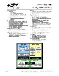
C8051F50x-F51x
12.2.1.3. Stack ............................................................................................ 99
13. Special Function Registers................................................................................. 100
13.1. SFR Paging ................................................................................................... 100
13.2. Interrupts and SFR Paging............................................................................ 100
13.3. SFR Page Stack Example............................................................................. 101
14. Interrupts .............................................................................................................. 117
14.1. MCU Interrupt Sources and Vectors.............................................................. 117
14.1.1. Interrupt Priorities.................................................................................. 118
14.1.2. Interrupt Latency ................................................................................... 118
14.2. Interrupt Register Descriptions...................................................................... 120
14.3. External Interrupts INT0 and INT1................................................................. 126
15. Flash Memory....................................................................................................... 129
15.1. Programming The Flash Memory.................................................................. 129
15.1.1. Flash Lock and Key Functions.............................................................. 129
15.1.2. Flash Erase Procedure ......................................................................... 129
15.1.3. Flash Write Procedure .......................................................................... 130
15.1.4. Flash Write Optimization....................................................................... 130
15.2. Non-volatile Data Storage ............................................................................. 131
15.3. Security Options ............................................................................................ 131
15.4. Flash Write and Erase Guidelines................................................................. 133
15.4.1. V Maintenance and the V monitor ................................................ 133
DD
DD
15.4.2. PSWE Maintenance.............................................................................. 133
15.4.3. System Clock ........................................................................................ 134
16. Power Management Modes................................................................................. 138
16.1. Idle Mode....................................................................................................... 138
16.2. Stop Mode ..................................................................................................... 139
16.3. Suspend Mode .............................................................................................. 139
17. Reset Sources...................................................................................................... 141
17.1. Power-On Reset............................................................................................ 142
17.2. Power-Fail Reset/VDD Monitor ..................................................................... 142
17.3. External Reset............................................................................................... 144
17.4. Missing Clock Detector Reset ....................................................................... 144
17.5. Comparator0 Reset ....................................................................................... 145
17.6. PCA Watchdog Timer Reset ......................................................................... 145
17.7. Flash Error Reset .......................................................................................... 145
17.8. Software Reset.............................................................................................. 145
18. External Data Memory Interface and On-Chip XRAM....................................... 147
18.1. Accessing XRAM........................................................................................... 147
18.1.1. 16-Bit MOVX Example .......................................................................... 147
18.1.2. 8-Bit MOVX Example ............................................................................ 147
18.2. Configuring the External Memory Interface................................................... 148
18.3. Port Configuration.......................................................................................... 148
18.4. Multiplexed and Non-multiplexed Selection................................................... 153
18.4.1. Multiplexed Configuration...................................................................... 153
18.4.2. Non-multiplexed Configuration.............................................................. 154
4
Rev. 1.1

 SILICON [ SILICON ]