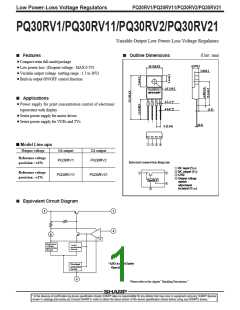
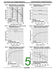
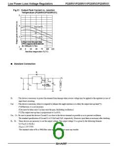
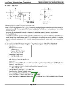
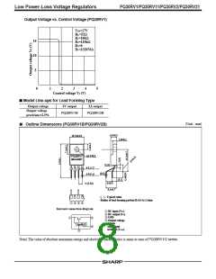
Low Power-Loss Voltage Regulators
PQ30RV1/PQ30RV11/PQ30RV2/PQ30RV21
■ Absolute Maximum Ratings
(Ta=25˚C)
Parameter
Symbol
Rating
Unit
V
V
*1
VIN
Input voltage
35
7
*1
V
ADJ
Output voltage adjustment voltage
PQ30RV1/PQ30RV11
PQ30RV2/PQ30RV21
Power dissipation (No heat sink)
1
2
1.5
15
18
I
O
Output current
A
P
D1
D2
W
W
PQ30RV1/PQ30RV11
PQ30RV2/PQ30RV21
Power dissipation
P
(With infinite heat sink)
Junction temperature
Operating temperature
Storage temperature
Soldering temperature
*2
T
j
150
˚C
˚C
˚C
˚C
T
opr
-20to+80
-40to+150
260 (For 10s)
T
T
stg
sol
*1
*2
All are open except GND and applicable terminals.
Overheat protection may operate at T >=125˚C.
j
■ Electrical Characteristics
Unless otherwise specified, condition shall be
V
V
IN=15V, V
IN=15V, V
O
=10V, I
=10V, I
O
=0.5A, R
=1.0A, R
1
=390Ω (PQ30RV1/PQ30RV11)
O
O
1=390Ω (PQ30RV2/PQ30RV21)
(T
a
=25˚C)
Parameter
Symbol
Conditions
-
MIN.
4.5
TYP.
-
MAX.
Unit
V
Input voltage
VIN
35
PQ30RV1/PQ30RV2
PQ30RV11/PQ30RV21
PQ30RV1/PQ30RV11
PQ30RV2/PQ30RV21
R
R
2
2
=94Ω to 8.5kΩ
=84Ω to 8.7kΩ
=5mA to 1A
=5mA to 2A
Output voltage
V
V
O
1.5
-
30
IO
-
-
-
0.3
0.5
0.5
55
65
1.25
1.25
±1.0
1.0
1.0
2.5
-
Load regulation
Line regulation
Ripple rejection
%
%
Reg
L
IO
V
C
C
IN=11 to 28V
ref=0
ref=3.3µF
Reg
I
45
55
1.20
1.225
-
Fefer to Fig. 2
dB
RR
-
PQ30RV1/PQ30RV2
PQ30RV11/PQ30RV21
Temperature coefficient of reference voltage
1.30
1.275
-
Reference voltage
-
V
%
V
ref
ref
T
j
=0 to 125˚C
T
c
V
PQ30RV1/PQ30RV11
Dropout voltage
*3, I
*3, I
O
=0.5A
=2A
V
V
i
-
O
-
-
-
-
0.5
7
PQ30RV2/PQ30RV21
O
Quiescent current
IO
=0
mA
I
q
*3
Input voltage shall be the value when output voltage is 95% in comparison with the initial value.
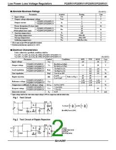
Fig.1 Test Circuit
VIN
47µF
VO
1●
2●
4●
R
2
1
R
R
2
R2
R
I
O
A
VO=Vref X 1+ --------- =1.25X 1+ ---------
1
1
+
3●
V
V
ref
R
0.33µF
[R1=390Ω,Vref =1.25V]
RL
V
A
I
q 390Ω
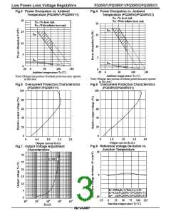
Fig.2 Test Circuit of Ripple Rejection
+
47µF
1●
2●
4●
e
i
~
+
R
2
I
O
=0.5A
f=120Hz (sine wave)
=0.5Vrms
RR=20 log (e
IO
+
3●
V eo
~
e
i
V
IN
Cref
R1
3.3µF
0.33µF
i/eo)
R
L
390Ω

 SHARP [ SHARP ELECTRIONIC COMPONENTS ]