15MHz, High Output Drive, High Precision,
Low Noise, Automotive Operational Amplifier
SGM8557H-1AQ
APPLICATIONS INFORMATION (continued)
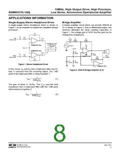
Cancel Input Capacitance
Input Current-Limit Protection
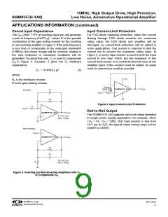
The CIN (20pF TYP) at inverting input pin will generate
a pole at frequency (2πR′CIN)-1, where R′ is the parallel
combination of the gain-setting resistor for the inverting
or non-inverting amplifier in Figure 3. If the pole-frequency
is less than or comparable to the unity-gain bandwidth
(15MHz), the phase margin will be reduced, ringing in
the step response or sustained oscillation will be
generated. To cancel this pole, CF is used to compensate
CIN in Figure 3. Equation 3 gives the CF feedback
capacitance.
For ESD diode clamping protection, when the current
flowing through ESD diode exceeds the maximum
rating value, the ESD diode and amplifier will be
damaged, so current-limit protection will be added in
some applications. One resistor is selected to limit the
current not to exceed the maximum rating value. In
Figure 4, a series input resistor is used to limit the input
current to less than 10mA, but the drawback of this
current-limit resistor is to contribute thermal noise at the
amplifier input. If this resistor must be added, its value
must be selected as small as possible.
CF = 8×(R/RF) pF
(3)
where:
+VS
RF is the feedback resistor.
R is the gain-setting resistor.
_
IOVERLOAD
10mA MAX
VOUT
SGM8557H-1AQ
CF
RF
Inverting
VIN
+
Figure 4. Input Current-Limit Protection
R
_
VIN
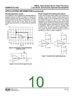
Rail-to-Rail Output
VOUT
R’ = R | | RF
SGM8557H-1AQ
The SGM8557H-1AQ supports rail-to-rail output operation.
In single power supply application, for example, when
+VS = 5V, -VS = GND, 2kΩ load resistor is tied from
OUT pin to VS/2, the typical output swing range is from
0.008V to 4.992V.
+
RFCF = RCIN
Non-Inverting
VIN
+
SGM8557H-1AQ
_
VOUT
RF
CF
R’ = R | | RF
RFCF = RCIN
R
Figure 3. Inverting and Non-Inverting Amplifiers with CF
to Compensate CIN
SG Micro Corp
www.sg-micro.com
MAY 2022
9

 SGMICRO [ Shengbang Microelectronics Co, Ltd ]