15MHz, High Output Drive, High Precision,
Low Noise, Automotive Operational Amplifier
SGM8557H-1AQ
APPLICATIONS INFORMATION (continued)
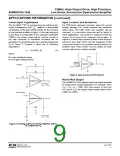
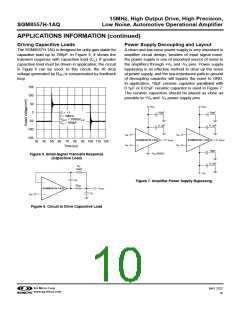
Driving Capacitive Loads
Power Supply Decoupling and Layout
The SGM8557H-1AQ is designed for unity-gain stable for
capacitive load up to 780pF. In Figure 5, it shows the
transient response with capacitive load (CL). If greater
capacitive load must be driven in application, the circuit
in Figure 6 can be used. In this circuit, the IR drop
voltage generated by RISO is compensated by feedback
loop.
A clean and low noise power supply is very important in
amplifier circuit design, besides of input signal noise,
the power supply is one of important source of noise to
the amplifiers through +VS and -VS pins. Power supply
bypassing is an effective method to clear up the noise
at power supply, and the low impedance path to ground
of decoupling capacitor will bypass the noise to GND.
In application, 10μF ceramic capacitor paralleled with
0.1μF or 0.01μF ceramic capacitor is used in Figure 7.
The ceramic capacitors should be placed as close as
possible to +VS and -VS power supply pins.
150
100
50
+VS
+VS
0
-50
10μF
10μF
G = +1
f = 10kHz
V
OUT = 100mVP-P
CL = 780pF
0.1μF
0.1μF
-100
-150
_
_
VN
VP
VN
VP
SGM8557H-1AQ
VOUT
SGM8557H-1AQ
VOUT
30 40 50 60 70 80 90 100 110 120
+
+
Time (μs)
10μF
-VS (GND)
Figure 5. Small-Signal Transient Response
(Capacitive Load)
0.1μF
RF
10kΩ
-VS
CF
Figure 7. Amplifier Power Supply Bypassing
_
RISO
SGM8557H-1AQ
VOUT
CL
VIN
+
Figure 6. Circuit to Drive Capacitive Load
SG Micro Corp
www.sg-micro.com
MAY 2022
10

 SGMICRO [ Shengbang Microelectronics Co, Ltd ]