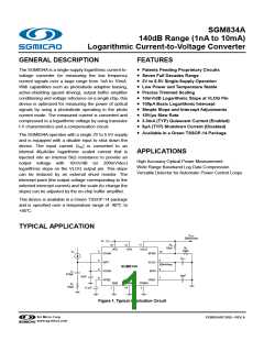
140dB Range (1nA to 10mA)
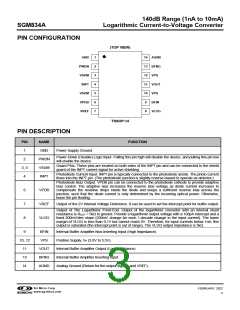
SGM834A
Logarithmic Current-to-Voltage Converter
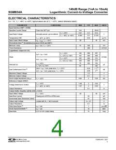
ELECTRICAL CHARACTERISTICS
(VP = 5V, TJ = -40℃ to +85℃, typical values are at TJ = +25℃, unless otherwise noted.)
PARAMETER
Input Interface (INPT, VSUM)
Specified Current Range
CONDITIONS
MIN
TYP
MAX
UNITS
Flows into INPT pin
1nA
0.47
10mA
0.53
0.5
0.5
TJ = +25℃
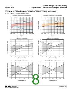
Input Node Voltage
Internally preset; can be altered
V
0.465
0.535
TJ = -40℃ to +85℃
Temperature Drift
0.02
TJ = -40℃ to +85℃
VIN - VSUM, TJ = +25℃
mV/℃
Input Guard Offset Voltage
Photodiode Bias (1) (Established between VPDB and INPT)
-20
70
20
mV
Minimum Value
100
300
mV
IPD = 1nA, TJ = +25℃
Trans-Resistance
mV/mA
Logarithmic Output (VLOG)
194
192
192
189
70
200
200
200
200
100
207
209
212
214
130
140
1.1 (3)
2 (3)
TJ = +25℃
1μA < IPD < 1mA
1nA < IPD < 1μA
TJ = 0℃ to +70℃
TJ = +25℃
Slope
mV/dec
TJ = 0℃ to +70℃
TJ = +25℃
Intercept (IZ)
pA
dB
60
TJ = 0℃ to +70℃
0.05
0.08
1.6
0.1
5
10nA < IPD < 1mA, peak error, TJ = +25℃
1nA < IPD < 1mA, peak error, TJ = +25℃
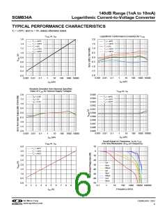
Law Conformance Error (2)
Maximum Output Voltage
Minimum Output Voltage
Shunt Output Resistance (ROUT
Reference Output (VREF)
V
V
)
4.95
5.05
kΩ
TJ = +25℃
1.98
1.97
2
2
2.02
2.03
TJ = +25℃
Voltage (Referred to AGND)
Output Resistance
V
TJ = -40℃ to +85℃
0.1
Ω
Output Buffer Amplifier (BFIN, BFNG, VOUT)
Input Offset Voltage
Input Bias Current
-20
20
mV
pA
GΩ
V
TJ = +25℃
Flowing out of BFIN or BFNG pins
20
25
Incremental Input Resistance (dv/di)
Output High Voltage
Output Resistance
Loaded with RL = 1kΩ to ground
VP - 0.1
0.1
Ω
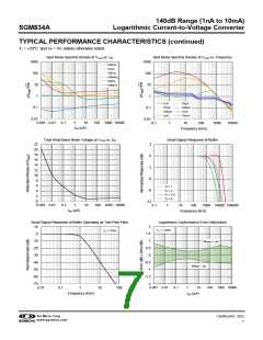
Wide-Band Noise (4)
Small Signal Bandwidth (4)
Slew Rate
IPD > 1μA
1
μV/√Hz
MHz
IPD > 1μA
10
0.2V to 4.8V output swing
15
V/μs
SG Micro Corp
www.sg-micro.com
FEBRUARY 2022
4

 SGMICRO [ Shengbang Microelectronics Co, Ltd ]