140dB Range (1nA to 10mA)
SGM834A
Logarithmic Current-to-Voltage Converter
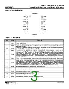
PIN CONFIGURATION
(TOP VIEW)
GND
1
2
3
4
5
6
7
14 AGND
13 BFNG
12 VPS
PWDN
VSUM
INPT
11 VOUT
10 VPS
VSUM
VPDB
VREF
9
8
BFIN
VLOG
TSSOP-14
PIN DESCRIPTION
PIN
1
NAME
GND
FUNCTION
Power Supply Ground.
Power-Down (Disable) Logic Input. Pulling this pin high will disable the device, and pulling this pin low
will enable the device.
2
PWDN
VSUM
INPT
Guard Pins. These pins are located on both sides of the INPT pin and can be connected to the shield
guard of the INPT current signal for active shielding.
3, 5
4
Photodiode Current Input. INPT pin is typically connected to the photodiode anode. The photo current
flows into the INPT pin. (The photodiode junction is slightly reverse biased to operate as detector.)
Photodiode Bias Output. VPDB pin can be connected to the photodiode cathode to provide adaptive
bias control. The adaptive bias increases the reverse bias voltage as diode current increases to
compensate the resistive drops inside the diode and keeps a sufficient reverse bias across the
junction, such that the diode current is only determined by the incoming optical power. Otherwise,
leave the pin floating.
6
7
8
VPDB
VREF
VLOG
Output of the 2V Internal Voltage Reference. It can be used to set the intercept point for buffer output.
Output of The Logarithmic Front-End. Output of the logarithmic converter with an internal shunt
resistance is ROUT = 5kΩ to ground. Provide a logarithmic output voltage with a 100pA intercept and a
fixed 200mV/dec slope (200mV change for each 1-decade change in the input current). The lower
margin of VLOG is less than 0.1V but cannot reach 0V. Therefore, for input currents below 1nA, this
output is saturated (the intercept point is out of range). The VLOG output impedance is 5kΩ.
9
10, 12
11
BFIN
VPS
Internal Buffer Amplifier Non-Inverting Input (High Impedance).
Positive Supply, VP (3.0V to 5.5V).
VOUT
BFNG
AGND
Internal Buffer Amplifier Output (Low Impedance).
Internal Buffer Amplifier Inverting Input.
13
I4
Analog Ground (Return for the output signals and VREF).
SG Micro Corp
FEBRUARY 2022
www.sg-micro.com
3

 SGMICRO [ Shengbang Microelectronics Co, Ltd ]