SX1231
ADVANCED COMMUNICATIONS & SENSING
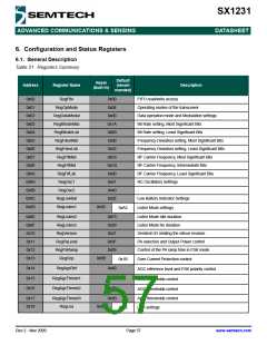
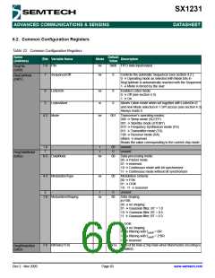
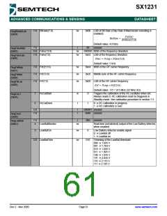
6. Configuration and Status Registers
DATASHEET
6.1. General Description
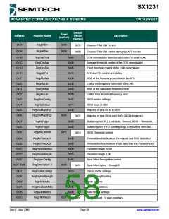
Table 21 Registers Summary
Default
Reset
Address
Register Name
(recom
Description
(built-in)
mended)
0x00
0x01
0x02
0x03
0x04
0x05
0x06
0x07
0x08
0x09
0x0A
0x0B
0x0C
0x0D
RegFifo
RegOpMode
RegDataModul
RegBitrateMsb
RegBitrateLsb
RegFdevMsb
RegFdevLsb
RegFrfMsb
RegFrfMid
0x00
FIFO read/write access
0x04
0x00
0x1A
0x0B
0x00
0x52
0xE4
0xC0
0x00
0x41
0x40
0x02
Operating modes of the transceiver
Data operation mode and Modulation settings
Bit Rate setting, Most Significant Bits
Bit Rate setting, Least Significant Bits
Frequency Deviation setting, Most Significant Bits
Frequency Deviation setting, Least Significant Bits
RF Carrier Frequency, Most Significant Bits
RF Carrier Frequency, Intermediate Bits
RF Carrier Frequency, Least Significant Bits
RC Oscillators Settings
RegFrfLsb
RegOsc1
RegOsc2
-
RegLowBat
RegListen1
Low Battery Indicator Settings
0x92
0xA2
Listen Mode settings
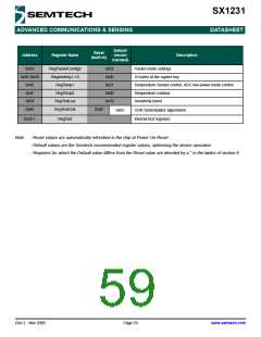
0x0E
0x0F
0x10
0x11
0x12
0x13
RegListen2
RegListen3
RegVersion
RegPaLevel
RegPaRamp
RegOcp
0xF5
0x20
0x21
0x9F
0x09
Listen Mode Idle duration
Listen Mode Rx duration
Semtech ID relating the silicon revision
PA selection and Output Power control
Control of the PA ramp time in FSK mode
0x0B
0x1B
Over Current Protection control
AGC reference level and FSK polarity control
AGC thresholds control
0x14
0x15
0x16
RegAgcRef
0x40
0xB0
0x7B
0x9B
RegAgcThresh1
RegAgcThresh2
AGC thresholds control
AGC thresholds control
LNA settings
0x17
0x18
RegAgcThresh3
RegLna
0x08
0x88
Rev 2 - Nov 2009
Page 57
www.semtech.com

 SEMTECH [ SEMTECH CORPORATION ]