SX1231
ADVANCED COMMUNICATIONS & SENSING
DATASHEET
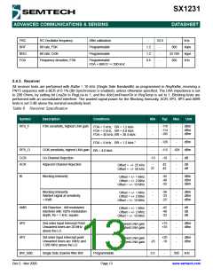
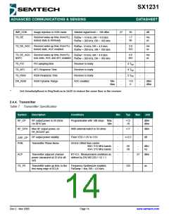
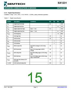
3. Chip Description
This section describes in depth the architecture of the SX1231 low-power, highly integrated transceiver.
3.1. Power Supply Strategy
The SX1231 employs an advanced power supply scheme, which provides stable operating characteristics over the full
temperature and voltage range of operation. This includes the full output power of +17dBm which is maintained from 1.8 to
3.6 V.
The SX1231 can be powered from any low-noise voltage source via pins VBAT1 and VBAT2. Decoupling capacitors should
be connected, as suggested in the reference design, on VR_PA, VR_DIG and VR_ANA pins to ensure a correct operation
of the built-in voltage regulators.
3.2. Low Battery Detector
A low battery detector is also included allowing the generation of an interrupt signal in response to passing a
programmable threshold adjustable through the register RegLowBat. The interrupt signal can be mapped to any of the DIO
pins, through the programmation of RegDioMapping.
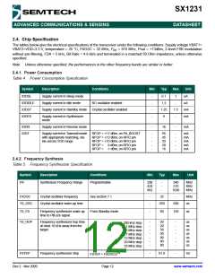
3.3. Frequency Synthesis
The LO generation on the SX1231 is based on a state-of-the-art fractional-N PLL. The PLL is fully integrated with
automatic calibration.
3.3.1. Reference Oscillator
The crystal oscillator is the main timing reference of the SX1231. It is used as a reference for the frequency synthesizer
and as a clock for the digital processing.
The XO startup time, TS_OSC, depends on the actual XTAL being connected on pins XTA and XTB. When using the built-
in sequencer, the SX1231 optimizes the startup time and automatically triggers the PLL when the XO signal is stable. To
manually control the startup time, the user should either wait for TS_OSC max, or monitor the signal CLKOUT which will
only be made available on the output buffer when a stable XO oscillation is achieved.
An external clock can be used to replace the crystal oscillator, for instance a tight tolerance TCXO. To do so, bit 4 at
address 0x59 should be set to 1, and the external clock has to be provided on XTA (pin 4). XTB (pin 5) should be left open.
The peak-peak amplitude of the input signal must never exceed 1.8 V. Please consult your TCXO supplier for an
appropriate value of decoupling capacitor, C .
D
XTA
OP
XTB
NC
TCXO
32 MHz
Vcc
GND
Vcc
CD
Figure 4. TCXO Connection
Rev 2 - Nov 2009
Page 16
www.semtech.com

 SEMTECH [ SEMTECH CORPORATION ]