SX1232
WIRELESS & SENSING
DATASHEET
Default
(recom
mended)
Reset
(built-in)
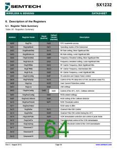
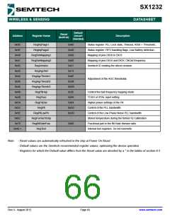
Address
Register Name
Description
0x3E
0x3F
0x40
0x41
0x42
0x43
0x44
0x45
0x46
0x4B
0x58
0x5A
0x5C
0x5E
0x6C
0x70
0x42 +
RegIrqFlags1
RegIrqFlags2
RegDioMapping1
RegDioMapping2
RegVersion
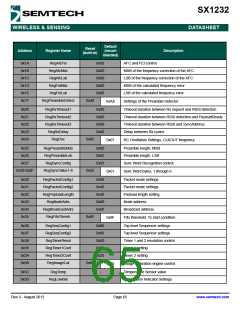
0x80
Status register: PLL Lock state, Timeout, RSSI > Threshold...
Status register: FIFO handling flags, Low Battery detection...
Mapping of pins DIO0 to DIO3
0x40
0x00
0x00
0x21
0x13
0x0E
0x5B
0xDB
0x2E
0x09
0x84
0xD0
0xD0
-
Mapping of pins DIO4 and DIO5, ClkOut frequency
Semtech ID relating the silicon revision
RegAgcRef
RegAgcThresh1
RegAgcThresh2
RegAgcThresh3
RegPllHop
Adjustment of the AGC thresholds
Control the fast frequency hopping mode
TCXO or XTAL input setting
RegTcxo
RegPaDac
Higher power settings of the PA
RegPll
Control of the PLL bandwidth
RegPllLowPn
RegFormerTemp
RegBitRateFrac
RegTest
Control of the Low Phase Noise PLL bandwidth
Stored temperature during the former IQ Calibration
Fractional part in the Bit Rate division ratio
Internal test registers. Do not overwrite
0x00
-
Note - Reset values are automatically refreshed in the chip at Power On Reset
- Default values are the Semtech recommended register values, optimizing the device operation
- Registers for which the Default value differs from the Reset value are denoted by a * in the tables of section 6.2
Rev 3 - August 2012
Page 66
www.semtech.com

 SEMTECH [ SEMTECH CORPORATION ]