SK4439
Anything to PECL Receiver
HIGH-PERFORMANCE PRODUCTS
Description
ꢀeatures
•
•
•
•
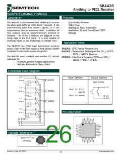
Quad Buffer/Receiver
3 GHz Fmax
Anything to PECL Translation
Available in 32 lead, 5mm X5mm, TQFP
Package
The SK4439 is an extremely fast, stable and accurate
low skew quad buffer or cable driver / receiver. It can
asychronously pass four distinct signals, or it can
resynchronize them to a common clock. In addition, all
four outputs may be asynchronously enabled or
disabled. All of the D flip-flops are triggered on the
rising edge of the CLK input. It is also capable of
receiving inputs of any technology or voltage level.
Application Notes
The SK4439 has 100Ω input termination resistors
across each of the four inputs to help reduce system
component count and increase integration.
AN1001 - EPIC Family Product Line
AN1003 - Termination Techniques for ECL / LVECL
PECL / LVPECL Devices
AN1004 - Interfacing Between LVDS and ECL /
LVECL / PECL / LVPECL
The SK4439 uses 50Ω outputs with sink/source
capability, and is optimized for applications that require:
• Point to point, double terminated, timing
critical lines
• Point to point, series terminated, timing
critical lines
Output Options
Input Options
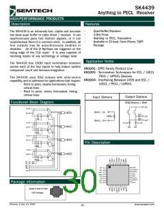
ꢀunctional Block Diagram
50Ω Source / Sink
VCC
IN0
1
OUT0
IN
<
0 - 3
>
>
IN0*
OUT0*
50Ω
D
Q
0
D* Q*
100
OUT
50Ω
*
OUT
IN<
0 - 3
*
IN1
10 mA
10 mA
1
0
OUT1
OUT1*
IN1*
VEE
VEE
D
Q
Q*
D*
IN2
1
0
OUT2
IN2*
OUT2*
Q
D
Pin Description
Q*
D*
IN3
1
0
OUT3
IN3*
OUT3*
D
Q
Q*
D*
CLK
CLK*
SEL*
SEL
EN
V
CC
V
CC
OUT1*
OUT1
SEL
EN*
SEL*
V
V
EE
EE
CLK*
CLK
OUT2
EN
OUT2*
EN*
Package Information
V
CC
V
CC
32 pin, 5 mm X 5 mm
TQFP Package
Revision 1/July 10, 2002
www.semtech.com
30

 SEMTECH [ SEMTECH CORPORATION ]