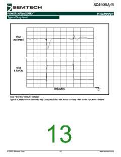
SC4905A/B
POWER MANAGEMENT
Application Information (Cont.)
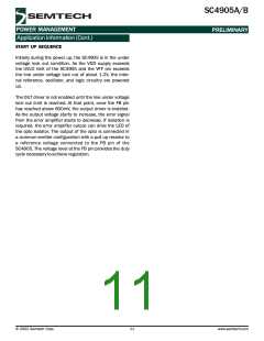
FEED BACK
PRELIMINARY
GATE DRIVERS
The error signal from the output of an external Error am- OUT is a CMOS gate drive output stage that is supplied
plifier such as SC431 or SC4431 is applied to the invert- from REF and provides a peak source/sink current of
ing input of the PWM comparator at the FB pin either about 1mA. The output stage is capable of driving the
directly or via an opto coupler for the Isolated applica- logic input of external MOSFET Drivers and is switched at
tions. For best stability keep the FB trace length as short the oscillator frequency. When the voltage on the RC pin
as possible.
is rising,, the output is high.
It should be noted that if high speed/high current drivers
such as the SC1301 are used, careful layout must be fol-
lowed in order to minimize stary inductance, which might
cause negative voltages at the output of the drivers. This
negative voltage can be clamped to reasonable level by
placing a small Schottky diode directly at the output of the
driver as shown below.
8
1
2
REF
7
4.7nF C36
Secondary Supply
Vout
R22
1.1k
22pF
C31
C33
R24
680pF
FB
6
5
3
4
C32
1nF
R25
C30
NA
3.74k
R29
NA
100k
R23
5.1k
R26
1
5
80.2k
MOCD207
4
C34
C35
22n, 16V
0.1u,16V
U6
SC4431
R27
9.1k
Vref
REF VDD
VDD
Mosfet Gate
2
0
R13
SC1301A
SC4905
U1
3
5
C17
C18
1
2
3
4
5
10
9
D8
The signal at the FB pin is then compared to the ramp
signal from the RC pin and the OUT gate drive signal is
generated.
VDD
REF
OUT
C22
1
FB
4
8
VFF
DMAX
RC
GND
ILIM
D11
2
7
U2
6
Voltages below 600mV at the FB pin, will produce a 0%
duty cycle at the OUT drive. Maximum duty cycle is pro-
duced when VFB-600mV>VFF. The FB signal range is from
600mv to 4V.
SYNC
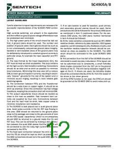
SOFT START
During start up of the converter, the discharged output
capacitor, and the load current demand large supply cur-
rent requirements. To avoid this a soft start scheme is
usually implemented where the duty cycle of the regula-
tor is gradually increased from 0% until the soft start
duration is elapsed.
OVER CURRENT
A pulse by pulse current limit is provided by the SC4905.
The current information is sensed at the ILIM pin and com-
pared to a peak current limit level of 200mV. If the 200mV
limit is exceeded, the OUT pulse is terminated.
Programmable soft start duration can implemented exter-
nally by utilizing a simple external circuitry shown below.
REF VDD
REF
SC4905
R13
U1
R22
0
SC4905
1.1k
1
VDD
FB
REF
OUT
U1
C17
6
3
4
2
3
4
5
9
8
7
6
1
2
3
4
5
10
9
VDD
FB
REF
OUT
C22
C30
M1
VFF
DMAX
RC
GND
ILIM
5
8
VFF
GND
ILIM
56.2K
7
R17
DMAX
RC
MOCD207
6
SYNC
SYNC
R30
Rsense
Csoft start
D7
C26
D15
R11
VDD
SC1301A
C18
3
5
Approximate soft start duration can be calculated as be-
low:
D8
1
4
D11
U2
T
≅ C
×R22
SoftStart
SoftStart
2
2002 Semtech Corp.
10
www.semtech.com

 SEMTECH [ SEMTECH CORPORATION ]