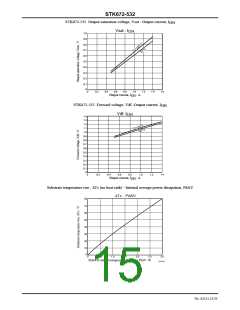
STK672-532
Usage Notes
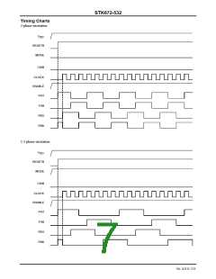
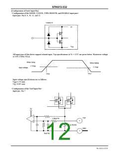
1. STK672-520, STK672-532 and STK672-540 input signal functions and timing
(All inputs have no internal pull-up resistor.)
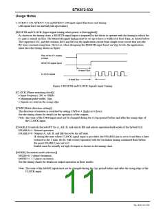
[RESETB and CLOCK (Input signal timing when power is first applied)]
As shown in the timing chart, a RESETB signal input is required by the driver to operate with the timing in which the
F1 gate is turned on first. The RESETB signal timing must be set up to have a width of at least 10μs, as shown below.
The capacitor CO2, and the resistors RO3 and RO4 in the application circuit form simple reset circuit that uses the
RC time constant rising time. However, when designing the RESETB input based on V levels, the application
IH
must have the timing shown in figure.
Rise of the 5V supply
voltage
RESETB signal input
At least 10μs
CLOCK signal
At least 5μs
Figure 1 RESETB and CLOCK Signals Input Timing
[CLOCK (Phase switching clock)]
• Input frequency: DC to 50kHz
• Minimum pulse width: 10μs
• Signals are read on the rising edge.
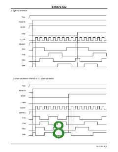
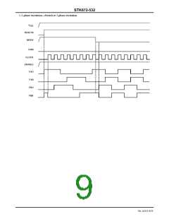
[CWB (Motor direction setting)]
The direction of rotation is switched by setting CWB to 1 (high) or 0 (low).
See the timing charts for details on the operation of the outputs.
Note: The state of the CWB input must not be changed during the 6.25μs period before and after the rising edge of
the CLOCK input.
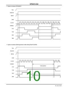
[ENABLE (Controls forced OFF for A, AB, B, and selects BB and selects operation/hold mode of the hybrid IC)]
ENABLE=1: Normal operation
ENABLE=0: Outputs A, AB, B, and BB forced to the off state.
If, during the state where CLOCK signal input is provided, the ENABLE pin is set to 0 and then is later
restored to the 1 state, the IC will resume operation with the excitation timing continued from before
the point ENABLE was set to 0.
Enable must be initially set high for input as shown in the timing chart.
[MODE (Excitation mode selection)]
MODE=0: 2-phase excitation
MODE=1: 1-2 phase excitation
See the timing charts for details on output operation in these modes.
Note: The state of the MODE input must not be changed during the 5μs period before and after the rising edge of the
CLOCK input.
No. A2111-11/23

 SANYO [ SANYO SEMICON DEVICE ]