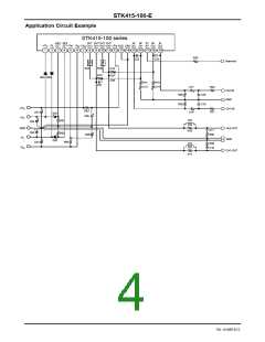
STK415-100-E
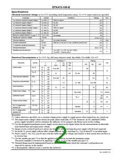
Specifications
Absolute maximum ratings at Ta=25°C (excluding rated temperature items), Tc=25°C unless otherwise specified
Parameter
Symbol
max (1)
max (2)
max (3)
max (1)
max (2)
max (3)
Conditions
Ratings
Unit
V
V
V
V
V
V
maximum quiescent supply voltage 1
maximum supply voltage 2
maximum supply voltage 3
maximum quiescent supply voltage 1
maximum supply voltage 2
maximum supply voltage 3
V
V
V
V
V
V
V
When no signal
65
57
46
42
37
29
60
V
H
H
H
L
H
H
H
L
R ≥6Ω
V
L
R ≥4Ω
V
L
When no signal
V
R ≥6Ω
V
L
L
L
R ≥4Ω
V
L
L
L
Maximum voltage between V
V
*4
-V max
L
No loading
V
H and
L
H
Standby pin maximum voltage
Thermal resistance
Vst max
θj-c
-0.3 to +5.5
1.8
V
Per power transistor
°C/W
°C
°C
°C
Junction temperature
Tj max
Tc max
Tstg
Both the Tj max and Tc max conditions must be met.
150
IC substrate operating temperature
Storage temperature
125
-30 to +125
Allowable load shorted time
*3
ts
V
P
= 39V, V = 29V, R =8Ω, f=50Hz,
L L
=60W, 1-channel active
H
O
0.3
s
Electrical Characteristics at Tc=25°C, R =8Ω (non-inductive load), Rg=600Ω, VG=40dB, VZ=15V
L
Conditions *1
Ratings
Parameter
Symbol
unit
W
V
f
P
THD
(%)
O
min
typ
max
(V)
(Hz)
(W)
Output power
P
(1)
(2)
V
H
39
29
O
20 to 20k
0.8
0.8
60
V
L
P
V
32
24
O
H
1k
R =4Ω
60
0.4
L
V
L
Total harmonic distortion
Frequency characteristics
Input impedance
THD
V
39
29
H
20 to 20k
60
1.0
1.0
%
Hz
V
L
f , f
V
39
29
L
H
H
+0 -3dB
20 to 50k
55
V
L
ri
V
39
29
H
1k
kΩ
V
L
Output noise voltage
Quiescent current
*2
V
V
47
31
NO
H
Rg=2.2kΩ
1.0
mVrms
mA
mV
V
V
L
I
V
47
31
30
CCO
H
R =∞
L
V
V
100
L
Output neutral voltage
V
47
31
N
H
-70
2.5
0
0
+70
0.6
V
L
Pin 17 voltage when
standby ON
VST ON
V
39
29
H
Standby
*7
*7
V
L
Pin 17 voltage when
standby OFF
VST OFF
V
39
29
H
Operating
3.0
V
V
L
[Remarks]
*1: Unless otherwise specified, use a constant-voltage power supply to supply power when inspections are carried out.
*2: The output noise voltage values shown are peak values read with a VTVM. However, an AC stabilized (50Hz)
power supply should be used to minimize the influence of AC primary side flicker noise on the reading.
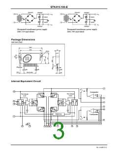
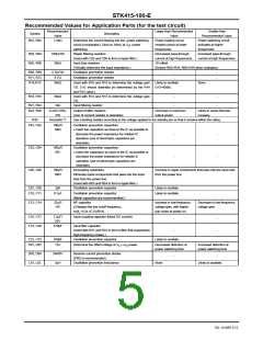
*3: Use the designated transformer power supply circuit shown in the figure below for the measurements of allowable
load shorted time and output noise voltage.
*4: Design circuits so that (|V |-|V |) is always less than 40V when switching the power supply with the load connected.
H L
*5: Set up the V power supply with an offset voltage at power supply switching (V -V ) of about 8V as an initial target.
L
L
O
*6: Please connect –Pre V
pin (#5 pin) with the stable minimum voltage and connect so that current does not flow in
CC
by reverse bias.
*7: Use the standby pin (pin 17) so that the applied voltage never exceeds the maximum rating.
The power amplifier is turned on by applying +2.5V to +5.5V to the standby pin (pin 17).
*8: Thermal design must be implemented based on the conditions under which the customer’s end products are
expected to operate on the market.
*9: A thermoplastic adhesive resin is used for this hybrid IC.
No. A1469-2/12

 SANYO [ SANYO SEMICON DEVICE ]