LA4628
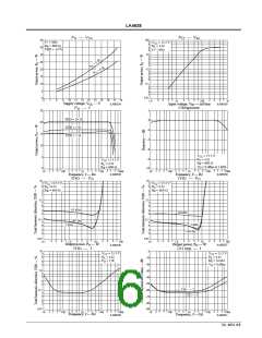
3. Impulse noise improvements
• While the LA4628 achieves a low level of impulse noise, if even further reductions in impulse noise at power on/off
(and when switching into or out of standby mode) a 0.47 µF capacitor may be inserted between pin 7 and the PRE
GND pin (pin 3). (Pin 7 is the output amplifier bias pin. Since the ability to withstand shorting the output pins to
V
CC
or ground is reduced for supply voltages over 16 V if the pin 7 capacitance is large, we recommend a value of
0.47 µF or lower for this capacitor.)
4. Protection circuits
• Due to the system structure of the protection circuit for shorts to V or ground, if there is a DC resistance between
CC
the amplifier output pins and ground, the protection circuit may operate when power is first applied and the
amplifier may fail to turn on. The basic design approach we recommend is not to adopt any designs in which there is
a DC resistance between the amplifier outputs and ground.
• The LA4628 includes a built-in thermal protection circuit to prevent the IC from being damaged or destroyed if
abnormally high temperatures occur. This thermal protection circuit gradually reduces the output if the IC junction
temperature (Tj) reaches the range 170 to 180°C due to inadequate heat sinking or other problem. If the temperature
falls, the amplifier will restart automatically.
• The LA4628 also includes other protection circuits. Use of these circuits also requires care during end product
design and testing.
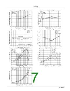
5. Other notes
• The LA4628 is a BTL power amplifier. When testing this device, the ground systems for the test equipment
connected to IC inputs, and that for the test equipment connected to IC outputs, must be isolated. Do not use a
common ground.
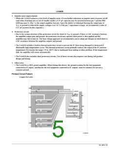
Printed Circuit Pattern
(copper foil side)
GND
C5
+
14
1
LA4628
C1
V
CC
IN1
+
+
C2
--OUT1
+OUT1
R2
R3
C6
C7
STB
C3
GND
R1
+
+
IN2
C4
+
C10
--OUT2
+OUT2
R4
R5
C8
C9
GND
ILA00349
No. 6632-5/8

 SANYO [ SANYO SEMICON DEVICE ]