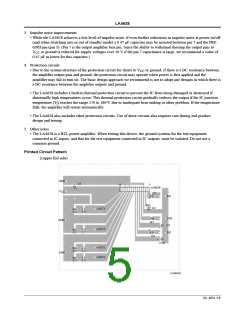
LA4628
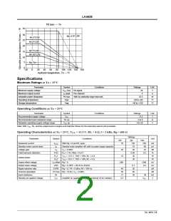
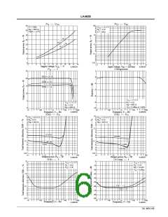
Pd max — Ta
35
30
25
θjc=2.0°C/W
θf=3°C/W
θf=4°C/W
20
15
θf=7°C/W
θf=10°C/W
10
5
No Fin
0
–20
0
20
40
60
80 100 120 140 160
Ambient temperature, Ta —°C
Specifications
Maximum Ratings at Ta = 25°C
Parameter
Maximum supply voltage
Maximum output current
Allowable power dissipation
Operating temperature
Storage temperature
Symbol
Conditions
Ratings
Unit
V
VCC max
No signal
24
4
I
O peak
Per channel
A
Pd max
Topr
With an arbitrarily large heat sink
32.5
–20 to +85
–40 to +150
W
°C
°C
Tstg
Operating Conditions at Ta = 25°C
Parameter
Symbol
VCC
Conditions
Ratings
13.5
Unit
V
Recommended supply voltage
Recommended load resistance range
Allowable operating supply voltage range
RL op
4 to 8
9 to 20
Ω
V
CC op
V
Note: With VCC, RL, and the output level in ranges such that the Pdmax for the heat sink used is not exceeded.
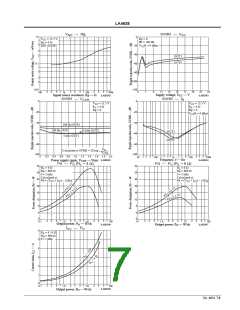
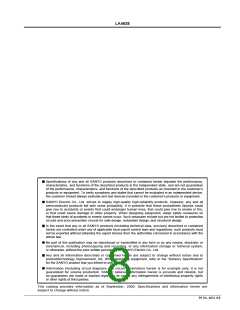
Operating Characteristics at Ta = 25°C, V = 13.5 V, RL = 4 Ω, f = 1 kHz, Rg = 600 Ω
CC
Ratings
typ
130
Parameter
Quiescent current
Symbol
Conditions
With Rg = 0 and RL open.
Unit
min
70
max
250
ICCO
Ist
mA
µA
dB
%
Standby mode current drain
Voltage gain
Standby mode (amplifier off), with no power supply capacitor.
VO = 0 dBm
10
40
60
42
VG
38
16
Total harmonic distortion
THD
PO1
PO2
PO = 1 W, Filter = FLAT
0.06
20
0.2
VCC = 13.5 V, THD = 10%, RL = 4 Ω
VCC = 16.5 V, THD = 10%, RL = 4 Ω
W
Output power
30
W
Output offset voltage
Output noise voltage
Ripple rejection ratio
Channel separation
Input resistance
V
N offset Rg = 0
VNO Rg = 0, BPF = 20 Hz to 20 kHz
SVRR Rg = 0, VR = 0 dBm, fR = 100 Hz
–300
+300
0.5
mV
mV
dB
dB
kΩ
V
0.1
50
60
30
40
50
CH Sep Rg = 10 kΩ, VO = 0 dBm
Ri
21
39
Standby pin applied voltage
VST
Amplifier on (applied through an external 10 kΩ resistor)
2.5
VCC
No. 6632-2/8

 SANYO [ SANYO SEMICON DEVICE ]