LA42102
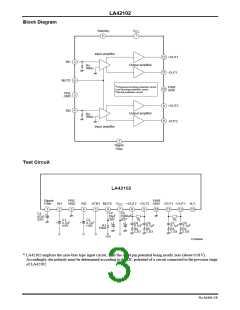
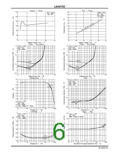
Block Diagram
Standby
5
V
CC
7
Input amplifier
+OUT1
12
IN1
2
Output amplifier
Ri=
30kΩ
11 -OUT1
PWR
MUTE
6
3
V
CC/ground shorting protection circuit
Load shorting protection circuit
Thermal protection circuit
10
GND
PRE
GND
+OUT2
-OUT2
8
9
4
IN2
Output amplifier
Ri=
30kΩ
Input amplifier
1
Ripple
Filter
Test Circuit
LA42102
Ripple
Filter
PRE
PWR
+OUT2 -OUT2 GND -OUT1 +OUT1 N.C.
IN1
2
GND
IN2
STBY MUTE
V
CC
1
3
4
5
6
7
8
9
10
11
12
13
C4
C5
C3
+
10µF
1000µF
47µF
/10V
/25V
R
C8
R
L
/25V
C1
C2
L
4.7µF
4.7µF
*
*
C9
C7
C6
+
+
R1
15kΩ
0.1µF 0.1µF
0.1µF 0.1µF
R3
2.2Ω
/10V
/10V
R4
2.2Ω
R5
2.2Ω
R2
2.2Ω
+5V
PCA00898
* LA42102 employs the zero-bias type input circuit, with the input pin potential being nearly zero (about 0.01V).
Accordingly, the polarity must be determined according to the DC potential of a circuit connected to the previous stage
of LA42102.
No.A0494-3/8

 SANYO [ SANYO SEMICON DEVICE ]