LA1245
Specifications
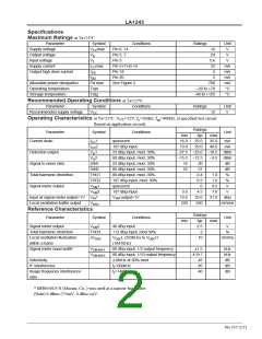
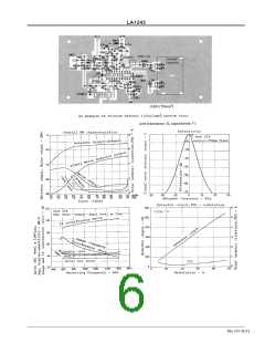
Maximum Ratings at Ta=25°C
Parameter
Symbol
Conditions
Ratings
Unit
V
Supply voltage
VCCmax
Pin 8, 14
16
24
5.6
32
5
Output voltage
V
o
Pin 5, 7
Pin 3
V
Input voltage
V
V
I
Supply current
ICCmax
Pin 5+7+8+14
Pin 18
mA
mA
mA
mA
°C
°C
Output high drive current
I
18
I
Pin 20
2
20
Pd max
Topr
Allowable power dissipation
Operating temperature
Storage temperature
See Figure 2
700
–20 to +70
Tstg
–40 to +125
Recommended Operating Conditions at Ta=25°C
Parameter
Symbol
Conditions
Ratings
12
Unit
V
Recommended supply voltage
VCC
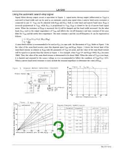
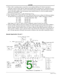
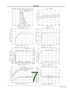
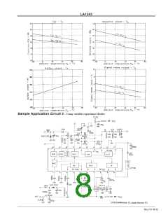
Operating Characteristics at Ta=25°C, V =12V, f =1MHz, f =400Hz, at specified test circuit
CC
r
m
(based on application circuit).
Ratings
typ
Parameter
Current drain
Symbol
Conditions
Unit
min
16.0
19.0
max
35.0
40.0
I
CC1
quiescent
25.0
mA
mA
ICC
2
107 dBµ input
29.0
Detection output
V 1
o
23 dBµ input, mod. 30%
80 dBµ input, mod. 30%
23 dBµ input, mod. 30%
80 dBµ input, mod. 30%
80 dBµ input, mod. 30%
–27.5 –23.0 –18.5 dBm
V 2
–15.5 –12.5
–9.5 dBm
o
Signal to noise ratio
Total harmonic distortion
Signal meter output
S/N1
S/N2
THD1
THD2
16
52
20
57
dB
dB
0.4
0.3
0
1.0
1.0
%
%
107 dBµ input, mod. 30%
quiescent
VSM
1
3
0.5
V
VSM
107 dBµ input
3.0
19.0
250
4.5
25.0
350
7.0
V
Input at signal meter output=1V VIN1
VSM output=1V
31.0
dBµ
mVrms
Local oscillation-buffer output
V
osc
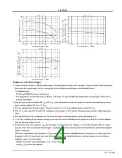
Reference Characteristics
Ratings
typ
Parameter
Symbol
Conditions
Unit
min
max
Signal meter output
V
SM2
40 dBµ input
2.5
V
%
Total harmonic distortion
Local oscillation fluctuation
within a band
THD3
112 dBµ input, mod.30%
2
∆V
V
L (522kHz) to V
osc
H
10
mVrms
osc
osc
(1647kHz)
Signal meter band width*
VSM-BW1
VSM-BW2
80 dBµ input, 1/2 output frequency
80 dBµ input, 1/10 output frequency
±10kHz at 30% mod.
±1.5
–4.5/+7
45
kHz
kHz
dB
Selectivity
IF interference
Image frequency interference
ratio
f =600kHz
r
85
dB
f =1400kHz
40
dB
r
* BFB450C4 N (Murata, Co.,) was used as a narrow band filter.
(Note) 0 dBm=775mV, 0 dBu=1µV.
No.737-2/11

 SANYO [ SANYO SEMICON DEVICE ]