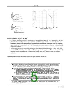
LA1143
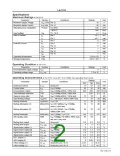
AC Test Circuit
T1 : CBTKAC-24782AUO (Toko Co.)
T2 : CBTKAE-24783X (Toko Co.)
22µH : S-220J (Korin Co.)
Input signal strength is an actual
input at pin 1.
Unit (resistance : Ω, capacitance : F)
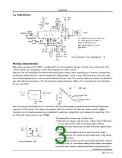
Muting Characteristic
The muting operation in the LA1143 is performed by an AF preamplifier, the gain of which varies continuously with
control current, and a muting drive circuit which supplies the control current.
The gain of th AF preamplifier decreases with increasing gain control current applied to pin 6. However, the gain does
not decrease further when the control current reaches approximately 120µA or more. The lower limit of the gain under
this condition depends upon a resistor connected between the pin 5 and GND, and the higher the resistance the lower the
gain (the higher the attenuation). Thus the maximum muting attenuation will be set by connecting the resistor between
the pin 5 and GND.
Since the muting control input pin 6 is connected to the base of the emitter-grounded transistor (through a protection
resistor of 500Ω in series), the voltage between pin 6 and GND is about 0.6V when the control current is applied.
In actual cases, the muting operation is accomplished by applying a voltage drive type muting drive output (pin 14) to
pin 6 through a high resistance (up to 20kΩ).
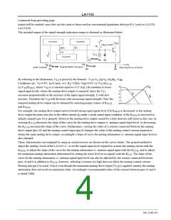
The muting drive output comes in three types :
1) Hole detector output which develops a voltage when C/N (carrier-
to-noise ratio) lowers under weak signal input condition.
2) A reversed output of the signal strength indicating output (output
at pin 15).
3) A bandwidth limited muting drive output which develops a
voltage when the AFC output becomes higher than ±V
detuning operation.
during
BE
All these outputs are led to an OR circuit and the processed output is
developed at pin 14. Of the above muting drive outputs, descriptions
on the hole detector output and the bandwidth limited muting drive
Continued on next page.
Unit (resistance : Ω)
No.1140-3/5

 SANYO [ SANYO SEMICON DEVICE ]