INSTRUCTION SET
S3C4510B
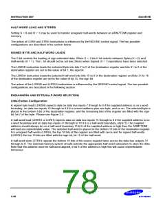
BLOCK DATA TRANSFER (LDM, STM)
The instruction is only executed if the condition is true. The various conditions are defined in Table 3-2. The
instruction encoding is shown in Figure 3-18.
Block data transfer instructions are used to load (LDM) or store (STM) any subset of the currently visible
registers. They support all possible stacking modes, maintaining full or empty stacks which can grow up or down
memory, and are very efficient instructions for saving or restoring context, or for moving large blocks of data
around main memory.
THE REGISTER LIST
The instruction can cause the transfer of any registers in the current bank (and non-user mode programs can also
transfer to and from the user bank, see below). The register list is a 16 bit field in the instruction, with each bit
corresponding to a register. A 1 in bit 0 of the register field will cause R0 to be transferred, a 0 will cause it not to
be transferred; similarly bit 1 controls the transfer of R1, and so on.
Any subset of the registers, or all the registers, may be specified. The only restriction is that the register list
should not be empty.
Whenever R15 is stored to memory the stored value is the address of the STM instruction plus 12.
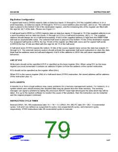
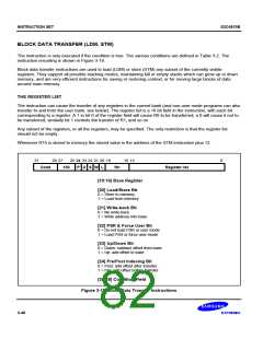
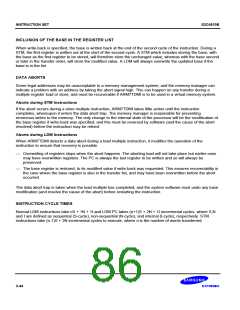
31
28 27
25 24 23 22 21 20 19
16 15
0
100
P U S W L
Rn
Register list
Cond
[19:16] Base Register
[20] Load/Store Bit
0 = Store to memory
1 = Load from memory
[21] Write-back Bit
0 = No write-back
1 = Write address into base
[22] PSR & Force User Bit
0 = Do not load PSR or user mode
1 = Load PSR or force user mode
[23] Up/Down Bit
0 = Down: subtract offset from base
1 = Up: add offset to base
[24] Pre/Post Indexing Bit
0 = Post: add offset after transfer
1 = Pre: add offset bofore transfer
[31:28] Condition Field
Figure 3-18. Block Data Transfer Instructions
3-40

 SAMSUNG [ SAMSUNG ]