S3C4510B
APPENDIX A
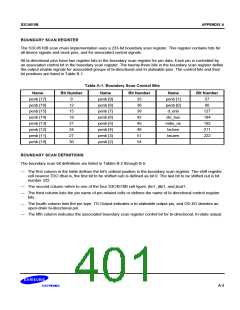
BOUNDARY SCAN REGISTER
The S3C4510B scan chain implementation uses a 233-bit boundary scan register. This register contains bits for
all device signals and clock pins, and for associated control signals.
All bi-directional pins have two register bits in the boundary scan register for pin data. Each pin is controlled by
an associated control bit in the boundary scan register. The twenty-three bits in the boundary scan register define
the output enable signals for associated groups of bi-directional and tri-stateable pins. The control bits and their
bit positions are listed in Table B-1.
Table A-1. Boundary Scan Control Bits
Name
Bit Number
Name
Bit Number
Name
penb [1]
penb [0]
d_enb
Bit Number
penb [17]
penb [16]
penb [15]
penb [14]
penb [13]
penb [12]
penb [11]
penb [10]
9
penb [9]
penb [8]
penb [7]
penb [6]
penb [5]
penb [4]
penb [3]
penb [2]
33
36
39
42
45
48
51
54
57
12
15
18
21
24
27
30
60
127
184
192
211
222
dis_bus
mdio_oe
txcben
txcaen
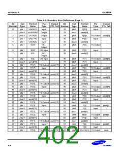
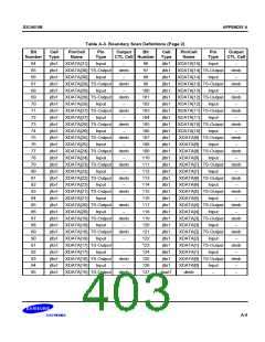
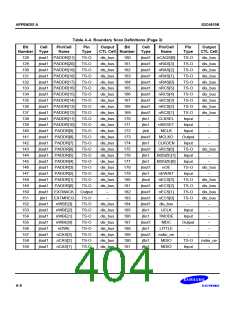
BOUNDARY SCAN DEFINITIONS
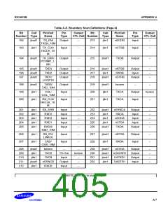
The boundary scan bit definitions are listed in Tables B-2 through B-5:
— The first column in the table defines the bit's ordinal position in the boundary scan register. The shift register
cell nearest TDO (that is, the first bit to be shifted out) is defined as bit 0. The last bit to be shifted out is bit
number 232.
— The second column refers to one of the four S3C4510B cell types: jtin1, jtbi1, and jtout1.
— The third column lists the pin name of pin-related cells or defines the name of bi-directional control register
bits.
— The fourth column lists the pin type. TS-Output indicates a tri-stateable output pin, and OD-I/O denotes an
open-drain bi-directional pin.
— The fifth column indicates the associated boundary scan register control bit for bi-directional, tri-state output.
A-3

 SAMSUNG [ SAMSUNG ]