S3C4510B
SYSTEM MANAGER
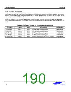
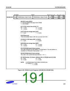
31 30 29
20 19
10 9
8
7
6
4
3
2
1
0
t
R
C
t
C
P
E
D
O
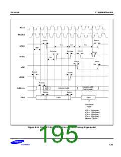
DRAM Bank # Next Pointer
DRAM Bank # Base Pointer
DRAMCON# CAN
tRP
Reserve
tCS
[0] EDO mode (EDO)
0 = Normal DRAM (Fast page mode DRAM)
1 = EDO DRAM
[2:1] CAS strobe time (tCS) (note)
00 = 1 cycle
01 = 2 cycles
10 = 3 cycles
11 = 4 cycles
[3:3] CAS pre-charge time (tCP)
0 = 1 cycle
1 = 2 cycles
[6:4] Reserved
These bits default value is 000. But, you must set to 001.
[7] RAS to CAS delay (tRC or tRCD)
0 = 1 cycle
1 = 2 cycles
[9:8] RAS pre-charge time (tRP)
00 = 1 cycle
10 = 3 cycles
01 = 2 cycles
11 = 4 cycles
[19:10] DRAM bank # base pointer
This value indicates the start address of DRAM bank #. The start address is
calculated as RAM bank # base pointer << 16
[29:20] DRAM bank # next pointer
This value is the current bank end address << 16 + 1
[31:30] Number of column address bits in DRAM bank # (CAN)
00 = 8 bits
01 = 9 bits
10 = 10 bits
11 = 11 bits
NOTE:
In SDRAM mode, this bit affect SDRAM cycle.
tCS value[1]: 0 = 1 cycle
1 = 2 cycle
Figure 4-29. DRAM Control Registers (DRAMCON–DRAMCON3)
4-49

 SAMSUNG [ SAMSUNG ]