MultiMediaCardTM
3 = stby
4 = tran
5 = data
6 = rcv
7 = prg
8 = dis
9–15 = reserved
‘0’ = not ready
‘1’ = ready
Permanently 0
‘0’ = disabled
‘1’ = enabled
8
EADY_FOR_DATA
SX
corresponds to buffer empty signaling on
the bus
A
C
7:6
5
reserved
APP_CMD
SR
The card will expect ACMD or indication
that the command has been interpreted
as ACMD.
4
reserved
Permanently 0
3:2
1:0
reserved for application specific commands
reserved for manufacturer test mode
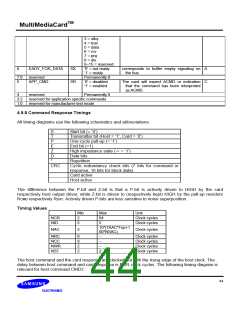
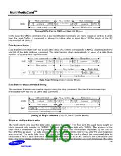
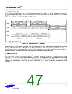
4.9.8 Command Response Timings
All timing diagrams use the following schematics and abbreviations:
S
Start bit (= ‘0’)
T
P
E
Transmitter bit (Host = ‘1’, Card = ‘0’)
One-cycle pull-up (= ‘1’)
End bit (=1)
Z
D
High impedance state (-> = ‘1’)
Data bits
*
Repetition
CRC
Cyclic redundancy check bits (7 bits for command or
response, 16 bits for block data)
Card active
Host active
The difference between the P-bit and Z-bit is that a P-bit is actively driven to HIGH by the card
respectively host output driver, while Z-bit is driven to (respectively kept) HIGH by the pull-up resistors
RCMD respectively RDAT. Actively driven P-bits are less sensitive to noise superposition.
Timing Values
Min
2
5
Max
64
5
Unit
Clock cycles
Clock cycles
NCR
NID
10*(TAAC*Fop+1
00*NSAC)
NAC
2
Clock cycles
NRC
NCC
NWR
NST
8
8
2
2
--
Clock cycles
Clock cycles
Clock cycles
Clock cycles
--
--
2
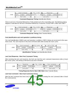
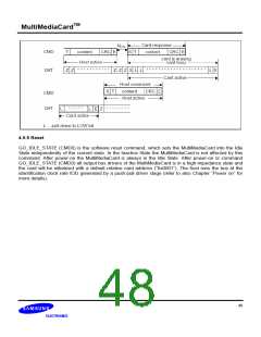
The host command and the card response are clocked out with the rising edge of the host clock. The
delay between host command and card response is NCR clock cycles. The following timing diagram is
relevant for host command CMD3 :
44

 SAMSUNG [ SAMSUNG ]