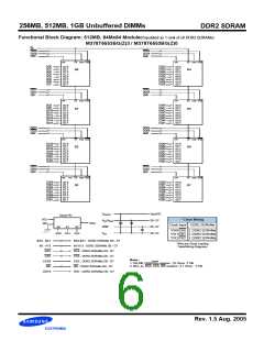
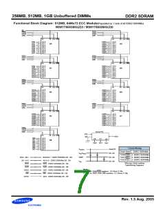
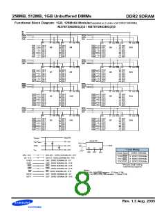
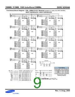
256MB, 512MB, 1GB Unbuffered DIMMs
DDR2 SDRAM
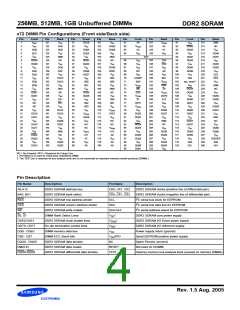
Input/Output Functional Description
Symbol
Type
Function
CK and CK are differential clock inputs. All the SDRAM addr/cntl inputs are sampled on the crossing of positive edge
of CK and negative edge of CK. Output (read) data is reference to the crossing of CK and CK (Both directions of
crossing)
CK0-CK2
CK0-CK2
Input
Activates the SDRAM CK signal when high and deactivates the CK Signal When low. By deactivating the clocks,
CKE low initiates the Powe Down mode, or the Self-Refresh mode
CKE0-CKE1
S0-S1
Input
Input
Enables the associated SDRAM command decoder when low and disables the command decoder when high. When
the command decoder is disbled, new command are ignored but previous operations continue. This signal provides
for external rank selection on systems with multiple ranks
RAS, CAS, WE
ODT0-ODT1
Input
Input
RAS, CAS, and WE (ALONG WITH CS) define the command being entered.
When high, termination resistance is enabled for all DQ, DQ and DM pins, assuming the function is enabled in the
Extended Mode Register Set (EMRS).
V
Supply
Supply
Input
Reference voltage for SSTL 18 inputs.
REF
Power supply for the DDR II SDRAM output buffers to provide improved noise immunity. For all current DDR2 unbuf-
fered DIMM designs, VDDQ shares the same power plane as VDD pins.
V
DDQ
BA0-BA1
A0-A13
Selects which SDRAM BANK of four is activated.
During a Bank Activate command cycle, Address input defines the row address (RA0-RA13)
During a Read or Write command cycle, Address input defines the colum address, In addition to the column address,
AP is used to invoke autoprecharge operation at the end of the burst read or write cycle. If AP is high, autoprecharge
is selected and BA0, BA1 defines the bank to be precharged. If AP is low, autoprecharge is disbled. During a pre-
charge command cycle, AP is used in conjunction with BA0, BA1 to control which bank(s) to precharge. If AP is high,
all banks will be precharged regardless of the state of BA0, BA1. If AP is low, BA0, BA1are used to define which bank
to precharge.
Input
DQ0-DQ63
CB0-CB7
In/Out
Input
Data and Check Bit Input/Output pins.
DM is an input mask signal for write data. Input data is masked when DM is sampled High coincident with that input
data during a write access. DM is sampled on both edges of DQS. Although DM pins are input only, the DM loading
matches the DQ and DQS loading.
DM0-DM8
Power and ground for DDR2 SDRAM input buffers, and core logic. VDD and VDDQ pins are tied to V /V
planes
DD DDQ
V
,V
Supply
In/Out
Input
DD SS
on these modules.
DQS0-DQS8
DQS0-DQS8
Data strobe for input and output data. For Rawcards using x16 orginized DRAMs DQ0-7 connect to the LDQS pin of
the DRAMs and DQ8-17 connect to the UDQS pin of the DRAM
These signals and tied at the system planar to either V or V
SS
to configure the serial SPD EERPOM address
DD
SA0-SA2
SDA
range.
This bidirectional pin is used to transfer data into or out of the SPD EEPROM. A resistor must be connected from the
SDA bus line to VDD to act as a pullup on the system board.
In/Out
Input
This signal is used to clock data into and out of the SPD EEPROM. A resistor may be connected from the SCL bus
time to VDD to act as a pullup onthe system board.
SCL
Power supply for SPD EEPROM. This supply is separate from the V /V
power plane. EEPROM supply is oper-
DD DDQ
V
SPD
Supply
DD
able from 1.7V to 3.6V.
Rev. 1.5 Aug. 2005
3-CD5/CC图片预览")
 SAMSUNG [ SAMSUNG ]