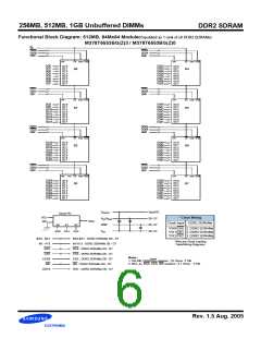
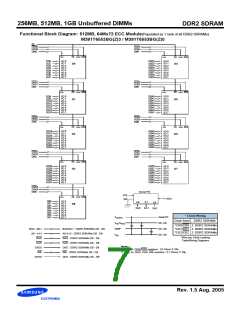
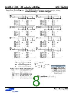
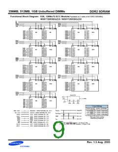
256MB, 512MB, 1GB Unbuffered DIMMs
DDR2 SDRAM
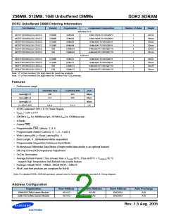
DDR2 Unbuffered DIMM Ordering Information
Part Number
Density
Organization
Component Composition
x64 Non ECC
Number of Rank
Height
M378T3354BG(Z)3-CD5/CC
M378T3354BG(Z)0-CD5/CC
M378T6553BG(Z)3-CD5/CC
M378T6553BG(Z)0-CD5/CC
M378T2953BG(Z)3-CD5/CC
M378T2953BG(Z)0-CD5/CC
256MB
256MB
512MB
512MB
1GB
32Mx64
32Mx64
64Mx64
64Mx64
128Mx64
128Mx64
32Mx16(K4T51163QB)*4
32Mx16(K4T51163QB)*4
64Mx8(K4T51083QB)*8
64Mx8(K4T51083QB)*8
64Mx8(K4T51083QB)*16
64Mx8(K4T51083QB)*16
1
1
1
1
2
2
30mm
30mm
30mm
30mm
30mm
30mm
1GB
x72 ECC
M391T6553BG(Z)3-CD5/CC
M391T6553BG(Z)0-CD5/CC
M391T2953BG(Z)3-CD5/CC
M391T2953BG(Z)0-CD5/CC
512MB
512MB
1GB
64Mx72
64Mx72
128Mx72
128Mx72
64Mx8(K4T51083QB)*9
64Mx8(K4T51083QB)*9
64Mx8(K4T51083QB)*18
64Mx8(K4T51083QB)*18
1
1
2
2
30mm
30mm
30mm
30mm
1GB
Note: “Z” of Part number(11th digit) stand for Lead-free products.
Note: “3” of Part number(12th digit) stand for Dummy Pad PCB products.
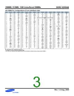
Features
•
Performance range
D5(DDR2-533)
CC(DDR2-400)
Unit
Speed@CL3
Speed@CL4
Speed@CL5
CL-tRCD-tRP
400
533
-
400
400
-
Mbps
Mbps
Mbps
CK
4-4-4
3-3-3
•
•
JEDEC standard 1.8V ± 0.1V Power Supply
= 1.8V ± 0.1V
V
DDQ
•
200 MHz f for 400Mb/sec/pin, 267MHz f for 533Mb/sec/pin
CK CK
•
•
•
•
•
•
•
•
•
•
•
4 Banks
Posted CAS
Programmable CAS Latency: 3, 4, 5
Programmable Additive Latency: 0, 1 , 2 , 3 and 4
Write Latency(WL) = Read Latency(RL) -1
Burst Length: 4 , 8(Interleave/nibble sequential)
Programmable Sequential / Interleave Burst Mode
Bi-directional Differential Data-Strobe (Single-ended data-strobe is an optional feature)
Off-Chip Driver(OCD) Impedance Adjustment
On Die Termination
Average Refresh Period 7.8us at lower than a T
85°C, 3.9us at 85°C < T
< 95 °C
CASE
CASE
- support High Temperature Self-Refresh rate enable feature
•
•
Package: 60ball FBGA - 64Mx8 , 84ball FBGA - 32Mx16
All of Lead-free products are compliant for RoHS
Note: For detailed DDR2 SDRAM operation, please refer to Samsung’s Device operation & Timing diagram.
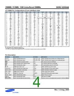
Address Configuration
Organization
Row Address
A0-A13
Column Address
A0-A9
Bank Address
BA0-BA1
Auto Precharge
64Mx8(512Mb) based Module
A10
32Mx16(512Mb) based Module
A0-A12
A0-A9
BA0-BA1
A10
Rev. 1.5 Aug. 2005
3-CD5/CC图片预览")
 SAMSUNG [ SAMSUNG ]