PDF
最近搜索
热门搜索
发布采购

| 型号: | K9K1208D0C |
| PDF下载: | 下载PDF文件 查看货源 |
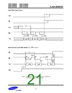
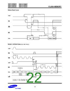
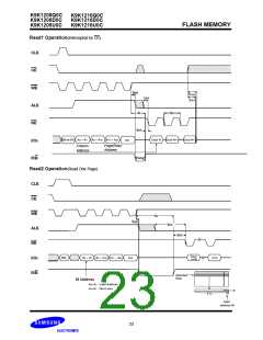
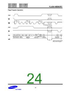
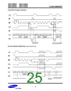
| 内容描述: | 64M ×8位, 32M x 16位NAND闪存 [64M x 8 Bit , 32M x 16 Bit NAND Flash Memory] |
| 分类和应用: | 闪存 |
| 文件页数/大小: | 39 页 / 955 K |
| 品牌: |  SAMSUNG [ SAMSUNG ] SAMSUNG [ SAMSUNG ] |
专业IC领域供求交易平台:提供全面的IC Datasheet资料和资讯,Datasheet 1000万数据,IC品牌1000多家。