K9F2808U0B-YCB0,YIB0
K9F2808Q0B-DCB0,DIB0
K9F2808U0B-VCB0,VIB0 K9F2808U0B-DCB0,DIB0
FLASH MEMORY
16M x 8 Bit Bit NAND Flash Memory
PRODUCT LIST
Part Number
K9F2808Q0B-D
K9F2808U0B-Y
K9F2808U0B-D
K9F2808U0B-V
Vcc Range
Organization
PKG Type
TBGA
1.7 ~ 1.9V
TSOP1
TBGA
X8
2.7 ~ 3.6V
WSOP1
FEATURES
· Voltage Supply
· Command/Address/Data Multiplexed I/O Port
· Hardware Data Protection
- Program/Erase Lockout During Power Transitions
· Reliable CMOS Floating-Gate Technology
- Endurance : 100K Program/Erase Cycles
- Data Retention : 10 Years
- K9F2808Q0B : 1.7~1.9V
- K9F2808U0B : 2.7 ~ 3.6 V
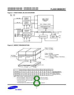
· Organization
- Memory Cell Array : (16M + 512K)bit x 8bit
- Data Register : (512 + 16)bit x8bit
· Automatic Program and Erase
- Page Program : (512 + 16)Byte
- Block Erase : (16K + 512)Byte
· 528-Byte Page Read Operation
- Random Access : 10ms(Max.)
- Serial Page Access
· Command Register Operation
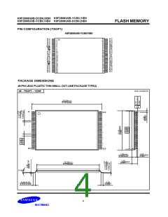
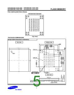
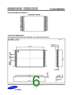
· Package
- K9F2808U0B-YCB0/YIB0 :
48 - Pin TSOP I (12 x 20 / 0.5 mm pitch)
- K9F2808X0B-DCB 0/ DIB0
63- Ball TBGA ( 9 x 11 /0.8mm pitch , Width 1.0 mm)
- K9F2808U0B-VCB0/VIB0
- K9F2808Q0B : 70ns
- K9F2808U0B : 50ns
· Fast Write Cycle Time
48 - Pin WSOP I (12X17X0.7mm)
* K9F2808U0B-V(WSOPI ) is the same device as
K9F2808U0B-Y(TSOP1) except package type.
- Program Time
- K9F2808Q0B : 300 ms(Typ.)
- K9F2808U0B : 200ms(Typ.)
- Block Erase Time : 2ms(Typ.)
GENERAL DESCRIPTION
The K9F2808X0B is a 16M(16,777,216)x8bit NAND Flash Memory with a spare 512K(524,288)x8bit. The device is offered in 1.8V or
3.3V Vcc. Its NAND cell provides the most cost-effective solution for the solid state mass storage market. A program operation pro-
grams the 528-byte page in typical 200ms and an erase operation can be performed in typical 2ms on a 16K-byte block. Data in a
page can be read out at 70ns/50ns(K9F2808Q0B:70ns, K9F2808U0B:50ns) cycle time per byte. The I/O pins serve as the ports for
address and data input/output as well as command input. The on-chip write control automates all program and erase functions
including pulse repetition, where required, and internal verification and margining of data. Even write-intensive systems can take
advantage of the K9F2808X0B’s extended reliability of 100K program/erase cycles by providing ECC(Error Correcting Code) with
real time mapping-out algorithm.
The K9F2808X0B is suitable for use in data memory of mobile communication system to reduce not only mount area but also power
consumption.
3

 SAMSUNG [ SAMSUNG ]