K4H561638D
DDR SDRAM
Notes 1. Includes ± 25mV margin for DC offset on VREF, and a combined total of ± 50mV margin for all AC noise and DC offset on
VREF, bandwidth limited to 20MHz. The DRAM must accommodate DRAM current spikes on VREF and internal DRAM noise
coupled TO VREF, both of which may result in VREF noise. VREF should be de-coupled with an inductance of ≤ 3nH.
2. V is not applied directly to the device. V is a system supply for signal termination resistors, is expected to be set equal to
TT
TT
VREF, and must track variations in the DC level of VREF
3. VID is the magnitude of the difference between the input level on CK and the input level on CK.
4. These parameters should be tested at the pin on actual components and may be checked at either the pin or the pad in
simulation. The AC and DC input specifications are relative to a VREF envelop that has been bandwidth limited to 200MHZ.
5. The value of VIX is expected to equal 0.5*VDDQ of the transmitting device and must track variations in the dc level of the same.
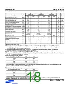
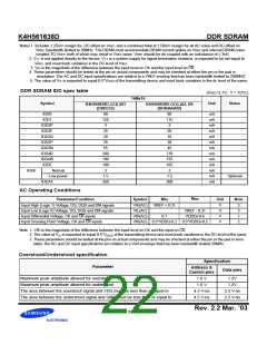
DDR SDRAM IDD spec table
(VDD=2.7V, T = 10°C)
16Mx16
Symbol
Unit
Notes
K4H560838D-GC(L)B3
(DDR333)
K4H560838D-GC(L)A2, B0
(DDR266A/B)
IDD0
IDD1
90
125
3
80
115
3
mA
mA
mA
mA
mA
mA
mA
mA
mA
mA
mA
mA
mA
IDD2P
IDD2F
IDD2Q
IDD3P
IDD3N
IDD4R
IDD4W
IDD5
25
20
20
18
35
30
55
45
200
190
180
3
170
155
165
3
IDD6
Normal
Low power
IDD7A
1.5
350
1.5
300
Optional
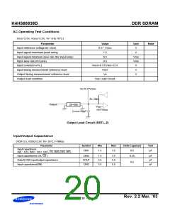
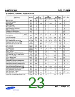
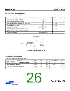
AC Operating Conditions
Max
Parameter/Condition
Symbol
Min
Unit
Note
Input High (Logic 1) Voltage, DQ, DQS and DM signals
Input Low (Logic 0) Voltage, DQ, DQS and DM signals.
Input Differential Voltage, CK and CK inputs
VIH(AC)
VIL(AC)
VID(AC)
VREF + 0.31
V
V
V
V
3
3
1
2
VREF - 0.31
VDDQ+0.6
0.7
Input Crossing Point Voltage, CK and CK inputs
VIX(AC) 0.5*VDDQ-0.2 0.5*VDDQ+0.2
Note 1. VID is the magnitude of the difference between the input level on CK and the input on CK.
2. The value of V is expected to equal 0.5*V of the transmitting device and must track variations in the DC level of the same.
IX
DDQ
3. These parameters should be tested at the pim on actual components and may be checked at either the pin or the pad in simu
lation. the AC and DC input specificatims are refation to a Vref envelope that has been bandwidth limited 20MHz.
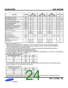
Overshoot/Undershoot specification
Specification
Parameter
Address &
Control pins
Data pins
Maximum peak amplitude allowed for overshoot
1.6 V
1.6 V
1.2V
1.2V
Maximum peak amplitude allowed for undershoot
The area between the overshoot signal and VDD must be less than or equal to
The area between the undershoot signal and GND must be less than or equal to
4.5 V-ns
4.5 V-ns
2.5 V-ns
2.5 V-ns
Rev. 2.2 Mar. ’03
- 22 -

 SAMSUNG [ SAMSUNG ]