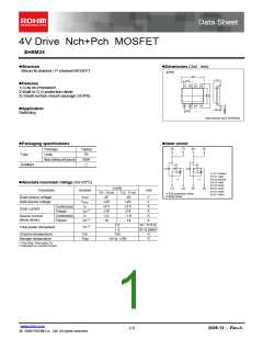
SH8M24
Data Sheet
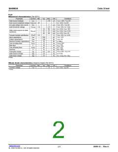
P-ch
Electrical characteristics (Ta=25C)
Parameter
Symbol Min. Typ. Max.
Conditions
μA VGS= 20V, VDS=0V
ID= −1mA, VGS=0V
μA VDS= −45V, VGS=0V
VDS= −10V, ID= −1mA
mΩ ID= −3.5A, VGS= −10V
mΩ ID= −3.5A, VGS= −4.5V
mΩ ID= −3.5A, VGS= −4V
Unit
Gate-source leakage
IGSS
−
−
−
10
−
Drain-source breakdown voltage V(BR) DSS −45
Zero gate voltage drain current
V
IDSS
−
−
−
−1
−2.5
63
84
92
−
−
−
−
−
Gate threshold voltage
VGS (th) −1.0
V
−
−
−
45
60
66
−
1700
200
135
16
17
70
14
Static drain-source on-state
resistance
∗
RDS (on)
∗
Forward transfer admittance
Input capacitance
Output capacitance
Reverse transfer capacitance
Turn-on delay time
Rise time
Yfs
Ciss
4.5
S
VDS= −10V, ID= −3.5A
−
−
−
−
−
−
−
−
pF
pF
pF
ns
ns
ns
ns
VDS= −10V
VGS=0V
Coss
Crss
td (on)
f=1MHz
∗
∗
∗
∗
∗
∗
∗
V
DD −25
V
I
D
= −2.0A
GS= −10V
=12.5Ω
=10Ω
t
r
−
−
−
V
Turn-off delay time
Fall time
td (off)
tf
R
L
R
G
Total gate charge
Gate-source charge
Qg
13.0 18.2
nC VDD −25V, VGS= −5V
nC ID= −3.5A
nC RL= 7.1Ω, RG= 10Ω
Qgs
Qgd
−
−
3.6
4.7
−
−
Gate-drain charge
∗ Pulsed
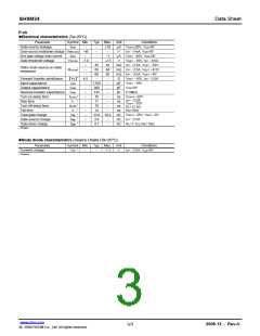
Body diode characteristics (Source-Drain) (Ta=25C)
Parameter
Symbol Min. Typ. Max.
Conditions
Unit
V
∗
Forward voltage
VSD
−
−
−1.2
IS= −3.5A, VGS=0V
∗ Pulsed
www.rohm.com
2009.12 - Rev.A
3/3
c
○ 2009 ROHM Co., Ltd. All rights reserved.

 ROHM [ ROHM ]