LM393DR/PWR/DGKR,LM2903DR/PWR/DGKR/VQDR/VQPWR
LM339DR/PWR,LM2901DR/PWR/VQDR/VQPWR
Technical Note
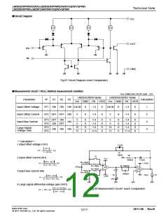
●Circuit Diagram
Vcc
OUT
IN+
IN-
GND
Fig.87 Circuit Diagram (each Comparator)
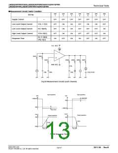
●Measurement circuit 1 NULL Method measurement condition
Vcc,GND,EK,VICR Unit:[V]
LM393/LM339 family
LM2903/LM2901 family
Parameter
VF
S1
S2
S3
Calculation
Vcc GND EK VICR Vcc GND EK VICR
Input Offset Voltage
Input Offset Current
Input Bias Current
VF1 ON ON ON 5 to 30
0
0
-1.4
-1.4
0
0
5 to 30
5
0
0
-1.4
-1.4
0
0
1
2
3
4
VF2 OFF OFF ON
5
VF3 OFF ON
ON
5
5
0
0
0
0
-1.4
-1.4
0
0
0
0
5
5
0
0
0
0
-1.4
-1.4
0
0
0
0
VF4 ON OFF
VF5
15
15
-1.4
15
15
-1.4
Large Signal
Voltage Gain
ON
ON
ON
VF6
-11.4
-11.4
-Calculation-
1.Input offset voltage (VIO)
0.1[μF]
VF1
1+ Rf /Rs
Vio
[V]
Rf
50[kΩ]
RK
500[kΩ]
S1
EK
2.Input offset current (IIO)
Vcc
0.1[μF]
VF2 - VF1
RS 50[Ω]
=
Iio
[A]
+15[V]
Ri(1+ Rf / Rs)
Ri 10[kΩ]
500[kΩ]
RK
=
VICR
DUT
Ri 10[kΩ]
=
NULL
S3
3.Input bias current (IIb)
RS 50[Ω]
=
1000[pF]
RL
VRL
-15[V]
V
VF
VF4 - VF3
2× Ri(1+ Rf / Rs)
GND
[A]
S2
Ib
50[kΩ]
4.Large signal differential voltage gain (AVD)
10× (1+ Rf /Rs)
AV 20× Log
Fig.88 Measurement Circuit1 (each Comparator)
[dB]
VF6 - VF5
www.rohm.com
© 2011 ROHM Co., Ltd. All rights reserved.
2011.06 - Rev.B
12/17

 ROHM [ ROHM ]