Datasheet
BR24G08-3
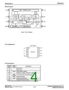
Block Diagram
8Kbit
EEPROM Array
A0
1
8
VCC
8bit
Address
Decoder
Word
Data
10bit
WP
A1
A2
2
3
4
7
6
5
Address Register
Register
START
STOP
SCL
SDA
Control Circuit
ACK
High Voltage
Generating circuit
Power Source
GND
Voltage Detection
Figure 3. Block Diagram
Pin Configuration
(TOP VIEW)
VCC
8
7
1
2
A0
WP
A1
A2
BR24G08-3
3
4
6
5
SCL
SDA
GND
Pin Descriptions
Terminal Input/
Descriptions
Name
Output
Don’t use(1)
Don’t use(1)
A0
-
A1
-
Input
-
Input/
Output
Slave address setting
A2
Reference voltage of all input / output, 0V
Serial data input serial data output
GND
SDA
Serial clock input
SCL
WP
Input
Input
-
Write protect terminal
Connect the power source.
VCC
(1)Pins not used as device address may be set to any of High, Low, and High-Z states
www.rohm.com
TSZ02201-0R2R0G100190-1-2
09.Mar.2013 Rev.002
©2013 ROHM Co., Ltd. All rights reserved.
4/33
TSZ22111・15・001

 ROHM [ ROHM ]