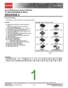
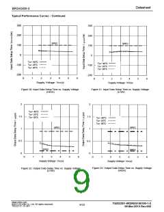
Datasheet
BR24G08-3
AC Characteristics (Unless otherwise specified, Ta=-40
℃
to +85℃, VCC=1.6V to 5.5V)
Limit
Parameter
Symbol
Unit
Min
-
Typ
Max
Clock Frequency
fSCL
tHIGH
tLOW
tR
-
-
-
-
-
-
-
-
-
-
-
-
-
-
-
-
-
-
-
400
kHz
µs
µs
µs
µs
µs
µs
µs
ns
ns
µs
µs
µs
µs
ms
µs
µs
µs
µs
Data Clock High Period
Data Clock Low Period
SDA, SCL (INPUT) Rise Time (1)
SDA, SCL (INPUT) Fall Time (1)
SDA (OUTPUT) Fall Time (1)
Start Condition Hold Time
Start Condition Setup Time
Input Data Hold Time
0.6
1.2
-
-
-
1.0
tF1
-
1.0
tF2
-
0.3
tHD:STA
tSU:STA
tHD:DAT
tSU:DAT
tPD
0.6
0.6
0
-
-
-
Input Data Setup Time
Output Data Delay Time
Output Data Hold Time
Stop Condition Setup Time
Bus Free Time
100
0.1
0.1
0.6
1.2
-
-
0.9
tDH
-
-
tSU:STO
tBUF
-
Write Cycle Time
tWR
5
0.1
-
Noise Spike Width (SDA and SCL)
WP Hold Time
tI
-
tHD:WP
tSU:WP
tHIGH:WP
1.0
0.1
1.0
WP Setup Time
-
WP High Period
-
(1) Not 100% TESTED.
Condition Input data level:VIL=0.2×Vcc VIH=0.8×Vcc
Input data timing reference level: 0.3×Vcc/0.7×Vcc
Output data timing reference level: 0.3×Vcc/0.7×Vcc
Rise/Fall time : ≦20ns
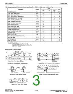
Serial Input / Output Timing
tR
tF1
tHIGH
70%
30%
70%
SCL
70% 70%
30%
70%
30%
30%
70%
tLOW
tHD:STA
tHD:DAT
tSU:DAT
70%
DATA(n)
70%
70%
DATA(1)
D0 ACK
70%
30%
70%
30%
ACK
D1
SDA
tDH
tPD
tBUF
(入力)
(INPUT)
tWR
70%
70%
30%
SDA
(出力)
(OUTPUT)
30%
30%
30%
30%
tF2
tSU:WP
tHD:WP
STOP CONDITION
○Input read at the rise edge of SCL
○Data output in sync with the fall of SCL
Figure 2-(d). WP Timing at Write Execution
Figure 2-(a). Serial Input / Output Timing
70%
DATA(n)
DATA(1)
D0
70%
70%
70%
D1
ACK
ACK
tSU:STA
tHD:STA
tSU:STO
tWR
tHIGH:WP
70%
70%
30%
30%
70%
STOP CONDITION
START CONDITION
Figure 2-(b). Start-Stop Bit Timing
Figure 2-(e). WP Timing at Write Cancel
70%
70%
ACK
D0
write data
(n-th address)
tWR
STOP CONDITION START CONDITION
Figure 2-(c). Write Cycle Timing
www.rohm.com
TSZ02201-0R2R0G100190-1-2
09.Mar.2013 Rev.002
©2013 ROHM Co., Ltd. All rights reserved.
3/33
TSZ22111・15・001

 ROHM [ ROHM ]