Datasheet
BR24G08-3
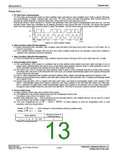
Timing Chart
1. I2C BUS Data Communication
I2C BUS data communication starts by start condition input, and ends by stop condition input. Data is always 8bit long,
and acknowledge is always required after each byte. I2C BUS carries out data transmission with several devices is
possible by connecting with 2 communication lines: serial data (SDA) and serial clock (SCL).
Among the devices, there should be a “master” that generates clock and control communication start and end. The rest
become “slave” which are controlled by an address peculiar to each device like this EEPROM. The device that outputs
data to the bus during data communication is called “transmitter”, and the device that receives data is called “receiver”.
SDA
1-7
1-7
1-7
8
9
8
9
8
9
SCL
S
P
START ADDRESS R/W
condition
ACK
DATA
ACK
DATA
ACK
STOP
condition
Figure 34. Data Transfer Timing
2. Start Condition (Start Bit Recognition)
(1) Before executing each command, start condition (start bit) where SDA goes from 'HIGH' down to 'LOW' when SCL is
'HIGH' is necessary.
(2) This IC always detects whether SDA and SCL are in start condition (start bit) or not, therefore, unless this condition is
satisfied, any command cannot be executed.
3. Stop Condition (Stop Bit Recongnition)
(1) Each command can be ended by a stop condition (stop bit) where SDA goes from Low to High while SCL is High.
4. Acknowledge (ACK) Signal
(1) The acknowledge (ACK) signal is a software rule to show whether data transfer has been made normally or not. In
master-slave communication, the device (Ex.µ-COM sends slave address input for write or read command to this IC)
at the transmitter (sending) side releases the bus after output of 8bit data.
(2) The device (Ex. This IC receives the slave address input of write or read command from the µ-COM) at the receiver
(receiving) side sets SDA 'LOW' during the 9th clock cycle, and outputs acknowledge signal (ACK signal) showing that
it has received the 8bit data.
(3) This IC, after recognizing start condition and slave address (8bit), outputs acknowledge signal (ACK signal) 'LOW'.
(4) After receiving 8bit data (word address and write data) during each write operation, this IC outputs acknowledge signal
(ACK signal) ‘LOW’.
(5) During read operation, this IC outputs 8bit data (read data), and detects acknowledge signal (ACK signal) 'LOW'.
When acknowledge signal (ACK signal) is detected, and stop condition is not sent from the master (µ-COM) side,
this IC continues to output data. When acknowledge signal (ACK signal) is not detected, this IC stops data transfer,
recognizes stop cindition (stop bit), and ends read operation. Then this IC becomes ready for another transmission.
5. Device Addressing
(1) Slave address comes after start condition from master.
(2) The significant 4 bits of slave address are used for recognizing a device type.
The device code of this IC is fixed to '1010'.
(3) Next slave addresses (A2 --- device address) are for selecting devices, and multiple devices can be used on a same
bus according to the number of device addresses.
(4) The most insignificant bit ( R / W --- READ / WRITE ) of slave address is used for designating write or read
operation, and is as shown below.
Setting R/ W to 0 ------- write (setting 0 to word address setting of random read)
Setting R/ W to 1 ------- read
Maximum number of
Slave address
Connected buses
1
0
1
0
A2 P1 P0 R/―W―
P0 and P1 are page select bits.
2
www.rohm.com
TSZ02201-0R2R0G100190-1-2
09.Mar.2013 Rev.002
©2013 ROHM Co., Ltd. All rights reserved.
13/33
TSZ22111・15・001

 ROHM [ ROHM ]