Daattaasshheeeett
BM2PXX2F
Operational Notes – continued
11. Unused Input Pins
Input pins of an IC are often connected to the gate of a MOS transistor. The gate has extremely high impedance and
extremely low capacitance. If left unconnected, the electric field from the outside can easily charge it. The small
charge acquired in this way is enough to produce a significant effect on the conduction through the transistor and
cause unexpected operation of the IC. So unless otherwise specified, unused input pins should be connected to the
power supply or ground line.
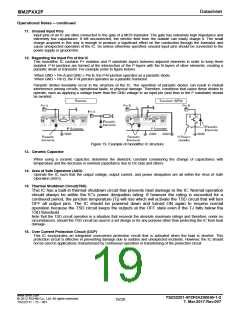
12. Regarding the Input Pin of the IC
This monolithic IC contains P+ isolation and P substrate layers between adjacent elements in order to keep them
isolated. P-N junctions are formed at the intersection of the P layers with the N layers of other elements, creating a
parasitic diode or transistor. For example (refer to figure below):
When GND > Pin A and GND > Pin B, the P-N junction operates as a parasitic diode.
When GND > Pin B, the P-N junction operates as a parasitic transistor.
Parasitic diodes inevitably occur in the structure of the IC. The operation of parasitic diodes can result in mutual
interference among circuits, operational faults, or physical damage. Therefore, conditions that cause these diodes to
operate, such as applying a voltage lower than the GND voltage to an input pin (and thus to the P substrate) should
be avoided.
Figure 19. Example of monolithic IC structure
13. Ceramic Capacitor
When using a ceramic capacitor, determine the dielectric constant considering the change of capacitance with
temperature and the decrease in nominal capacitance due to DC bias and others.
14. Area of Safe Operation (ASO)
Operate the IC such that the output voltage, output current, and power dissipation are all within the Area of Safe
Operation (ASO).
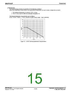
15. Thermal Shutdown Circuit(TSD)
This IC has a built-in thermal shutdown circuit that prevents heat damage to the IC. Normal operation
should always be within the IC’s power dissipation rating. If however the rating is exceeded for a
continued period, the junction temperature (Tj) will rise which will activate the TSD circuit that will turn
OFF all output pins. The IC should be powered down and turned ON again to resume normal
operation because the TSD circuit keeps the outputs at the OFF state even if the TJ falls below the
TSD threshold.
Note that the TSD circuit operates in a situation that exceeds the absolute maximum ratings and therefore, under no
circumstances, should the TSD circuit be used in a set design or for any purpose other than protecting the IC from heat
damage.
16. Over Current Protection Circuit (OCP)
This IC incorporates an integrated overcurrent protection circuit that is activated when the load is shorted. This
protection circuit is effective in preventing damage due to sudden and unexpected incidents. However, the IC should
not be used in applications characterized by continuous operation or transitioning of the protection circuit.
www.rohm.com
TSZ02201-0F2F0A200040-1-2
7. Mar.2017.Rev.007
© 2012 ROHM Co., Ltd. All rights reserved.
19/20
TSZ22111・15・001

 ROHM [ ROHM ]