Daattaasshheeeett
BHxxMA3 series
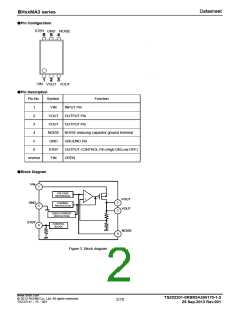
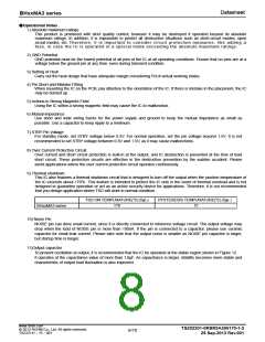
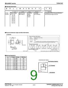
●Pin Configuration
STBY
GND NOISE
VIN
●Pin Description
VOUT VOUT
Pin No.
Symbol
Function
1
VIN
VOUT
VOUT
NOISE
GND
INPUT Pin
2
OUTPUT Pin
OUTPUT Pin
3
4
NOISE reducing capacitor ground terminal
GROUND Pin
5
6
STBY
FIN
OUTPUT CONTROL Pin (High:ON,Low:OFF)
OPEN
reverse
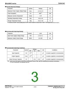
●Block Diagram
VIN
1
VOLTAGE
REFERENCE
-
+
VOUT
VOUT
GND
5
2
3
THERMAL
PROTECTION
OVER CURRENT
PROTECTION
STBY
6
CONTROL
BLOCK
NOISE
4
Figure 2. Block diagram
www.rohm.com
TSZ02201-0RBR0A300170-1-2
25.Sep.2013 Rev.001
© 2012 ROHM Co., Ltd. All rights reserved.
2/10
TSZ22111・15・001

 ROHM [ ROHM ]