Daattaasshheeeett
BHxxMA3 series
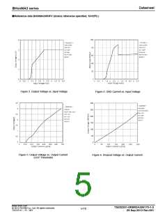
●About input/output capacitor
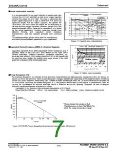
Capacity value of ceramic capacitor - DC bias characteristics
(Example)
It is recommended that an input capacitor is placed near pins
between the VCC pin and GND as well as an output capacitor
between the output pin and GND. The input is valid when the
power supply impedance is high or when the PCB trace has
significant length. For the output capacitor, the greater the
capacitance, the more stable the output will be depending on
the load and line voltage variations. However, please check the
actual functionality of this capacitor by mounting it on a board
for the actual application. Ceramic capacitors usually have
different, thermal and equivalent series resistance
characteristics, and may degrade gradually over continued
use.
10-V withstand voltage
B1characteristics
GRM188B11A105KA61D
10
0
10-V withstand voltage
B characteristics
-10
-20
-30
-40
-50
-60
-70
-80
-90
-100
6.3-V withstand voltage
B characteristics
10-V withstand voltage
F characteristics
4-V withstand voltage
X6S characteristics
10-V withstand voltage
F characteristics
0
0.5
1
1.5
2
2.5
3
3.5
4
For additional details, please check with the manufacturer,
and select the best ceramic capacitor for your application
DC Bias Voltage [V]
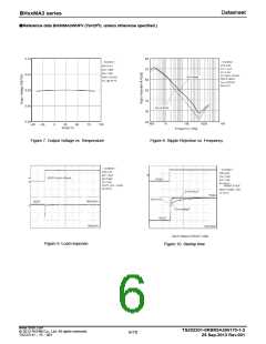
Figure 11. Capacity-bias characteristics
Cout=1.0μF,Cin=1.0μF,Temp=+25℃
●Equivalent Series Resistance (ESR) of a Ceramic Capacitor
100
Capacitors generally have ESR (equivalent series resistance) and it
operates stably in the ESR-IOUT area shown on the right. Since
ceramic capacitors, tantalum capacitors, electrolytic capacitors, etc.
generally have different ESR, please check the ESR of the capacitor to
be used and use it within the stability area range shown in the right
graph for evaluation of the actual application.
10
1
Stable region
0.1
0.01
0
50
100
150
200
250
300
Output CurrentꢀIOUTꢀ[mA]
Figure 12. Stable region (example)
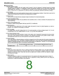
●Power Dissipation (Pd)
As for power dissipation, an estimate of heat reduction characteristics and internal power consumption of IC are shown, so
please use these for reference. Since power dissipation changes substantially depending on the implementation conditions
(board size, board thickness, metal wiring rate, number of layers and through holes, etc.), it is recommended to measure Pd
on a set board. Exceeding the power dissipation of IC may lead to deterioration of the original IC performance, such as
causing the operation of the thermal shutdown circuit or reduction in current capability. Therefore, be sure to prepare
sufficient margin within power dissipation for usage.
Calculation of the maximum internal power consumption of IC (PMAX)
PMAX=(VIN-VOUT)×IOMAX
Where : VIN=Input voltage
VOUT= Output voltage IOMAX: Maximum output current
0.8
0.7
0.6
0.5
0.4
0.3
0.2
0.1
0
0.68W
Standard ROHM
board
* Please design the margin so that
PMAX becomes is than Pd (PMAX<Pd)
within the usage temperature range
85
0
25
50
75
100
125
Ta (℃)
Figure 13.HVSOF6 Power dissipation heat reduction characteristics (Reference)
www.rohm.com
TSZ02201-0RBR0A300170-1-2
25.Sep.2013 Rev.001
© 2012 ROHM Co., Ltd. All rights reserved.
7/10
TSZ22111・15・001

 ROHM [ ROHM ]