BD9415FS
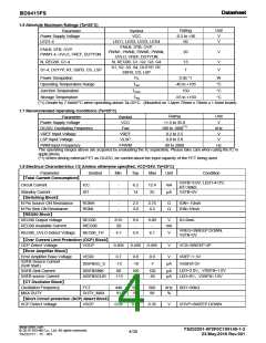
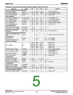
○PIN11, 14, 17, 20 :S1-S4, PIN23 : VREF
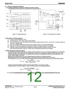
LED constant current driver is connected to the source of bill FET outside. Output current ILED is inversely proportional to
the resistance value. This is the input pin for analog dimming signal. Output current ILED is directly proportional to the
input voltage value. VREF pin is high impedance because the internal resistance is not connected to a certain bias.
Even if VREF function is not used, pin bias is still required because the open connection of this pin is not a fixed potential.
VREF pin voltage is set as 「VVREF」, LED current 「ILED」can be calculated as below.
VREF [V]
ILED[A]
0.2ꢀꢀ
RS[Ω]
ILED
LED
G
VREF 1.2V, RS 2[]
ILED 120[mA]ꢀ
+
-
S 240mV
RS
Figure 9. ILED setting example
For the adjustment of LED current with analog dimming by VREF, note that the output voltage of the DC/DC converter
largely changes accompanied by LED VF changes if the VREF voltage is changed rapidly. In particularly, when the VREF
voltages changed from high to low, it makes the LED terminal voltage seem higher transiently, which may influence
application such as activation of the LED short circuit protection. It needs to be adequately verified with an actual device
when analog dimming is used.
○PIN12, 15, 18, 21:LED1-LED4
LED constant current driver output pins. Drain of external NMOS is connected. Setting of LED current value is adjustable
by setting the VREF voltage and connecting a resistor to S pin. For details, see the explanation of <PIN:11, 14, 17, 20 S1
- S4, Pin23 : VREF >.
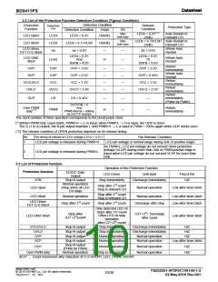
The abnormal voltage of this pin activates the protection function of LED OPEN detection, LED SHORT detection.
Please refer to < 2.2 List of The Protection Function Detection Condition> for details.
○PIN13, 16, 19, 22:G1-G4
This is the output terminal for driving the gate of the boost MOSFET. The high level
is REG90. Frequency can be set by the resistor connected to RT. Refer to <RT> pin description for the frequency setting.
○PIN24:LSP
LED Short detection voltage setting pin. Resistance voltage divider is internally on IC. It is set as 1.2V.
When need to establish the other voltage, use an external resistance voltage divider.
LSP pin voltage is set as LED SHORT PROTECTION detection voltage and can be calculated as below.
LEDSHORT 6.7VLSP[V]ꢀ
LEDSHORT:LSP detection voltage, VLSP:LSP pin voltage
Set LSP voltage in the range of 0.8V to 3.0V.
In addition to considering the voltage of the internal resistance voltage divider, it's necessary to establish the voltage of
the LSP terminal.
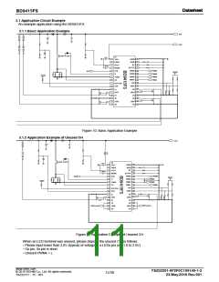
○PIN25, 26, 27, 28:PWM1-PWM4
These are the PWM dimming signal input terminals. The high / low level of PWM pins are the following.
State
PWM pin voltage
PWM= +1.5V to +18.0V
PWM= -0.3V to +0.8V
PWM=H
PWM=L
www.rohm.com
TSZ02201-0F2F0C100140-1-2
23.May.2016 Rev.001
© 2015 ROHM Co., Ltd. All rights reserved.
8/30
TSZ22111・15・001

 ROHM [ ROHM ]