BD9415FS
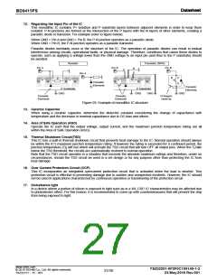
12. Regarding the Input Pin of the IC
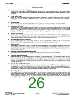
This monolithic IC contains P+ isolation and P substrate layers between adjacent elements in order to keep them
isolated. P-N junctions are formed at the intersection of the P layers with the N layers of other elements, creating a
parasitic diode or transistor. For example (refer to figure below):
When GND > Pin A and GND > Pin B, the P-N junction operates as a parasitic diode.
When GND > Pin B, the P-N junction operates as a parasitic transistor.
Parasitic diodes inevitably occur in the structure of the IC. The operation of parasitic diodes can result in mutual
interference among circuits, operational faults, or physical damage. Therefore, conditions that cause these diodes to
operate, such as applying a voltage lower than the GND voltage to an input pin (and thus to the P substrate) should
be avoided.
Resistor
Transistor (NPN)
Pin A
Pin B
Pin B
B
E
C
Pin A
B
C
E
P
P+
P+
N
P+
P
P+
N
N
N
N
N
N
N
Parasitic
Elements
Parasitic
Elements
P Substrate
GND GND
P Substrate
GND
GND
Parasitic
Elements
Parasitic
Elements
N Region
close-by
Figure 29. Example of monolithic IC structure
13. Ceramic Capacitor
When using a ceramic capacitor, determine the dielectric constant considering the change of capacitance with
temperature and the decrease in nominal capacitance due to DC bias and others.
14. Area of Safe Operation (ASO)
Operate the IC such that the output voltage, output current, and the maximum junction temperature rating are all
within the Area of Safe Operation (ASO).
15. Thermal Shutdown Circuit(TSD)
This IC has a built-in thermal shutdown circuit that prevents heat damage to the IC. Normal operation should always
be within the IC’s maximum junction temperature rating. If however the rating is exceeded for a continued period, the
junction temperature (Tj) will rise which will activate the TSD circuit that will turn OFF all output pins. When the Tj falls
below the TSD threshold, the circuits are automatically restored to normal operation.
Note that the TSD circuit operates in a situation that exceeds the absolute maximum ratings and therefore, under no
circumstances, should the TSD circuit be used in a set design or for any purpose other than protecting the IC from
heat damage.
16. Over Current Protection Circuit (OCP)
This IC incorporates an integrated overcurrent protection circuit that is activated when the load is shorted. This
protection circuit is effective in preventing damage due to sudden and unexpected incidents. However, the IC should
not be used in applications characterized by continuous operation or transitioning of the protection circuit.
17. Disturbance light
In a device where a portion of silicon is exposed to light such as in a WL-CSP, IC characteristics may be affected due
to photoelectric effect. For this reason, it is recommended to come up with countermeasures that will prevent the chip
from being exposed to light.
www.rohm.com
TSZ02201-0F2F0C100140-1-2
23.May.2016 Rev.001
© 2015 ROHM Co., Ltd. All rights reserved.
27/30
TSZ22111・15・001

 ROHM [ ROHM ]