BD9109FVM-LB
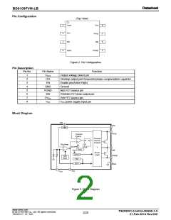
Pin Configuration
(Top View)
1
2
VOUT
ITH
VCC
PVCC
SW
8
7
6
3
4
EN
GND
PGND
5
Figure 2. Pin Configuration
Function
Pin Description
Pin No.
Pin Name
VOUT
ITH
1
2
3
4
5
6
7
8
Output voltage detect pin
GmAmp output pin/Connected phase compensation capacitor
Enable pin(Active High)
EN
GND
PGND
SW
Ground
Nch FET source pin
Pch/Nch FET drain output pin
Pch FET source pin
PVCC
VCC
VCC power supply input pin
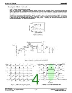
Block Diagram
EN
3
VCC
8
7
VREF
PVCC
Current
Comp.
Current
Sense/
Protect
R
Q
Gm Amp.
S
SLOPE
CLK
+
6
OSC
VCC
SW
Driver
Logic
UVLO
PGND
Soft
5
4
Start
TSD
SCP
GND
1
2
VOUT
ITH
Figure 3. Block Diagram
www.rohm.com
TSZ02201-0J4J0AJ00600-1-2
21.Feb.2014 Rev.002
© 2013 ROHM Co., Ltd. All rights reserved.
2/20
TSZ22111 • 15 • 001

 ROHM [ ROHM ]