3/4
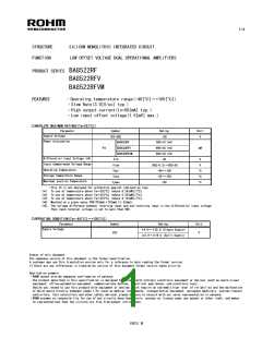
○ Physical Dimensions
8522
R
8
2
5
2
R
8522R
LOT No.
BA8522RF(SOP8) (単位:[mm])
BA8522RFV(SSOP-B8) (単位:[mm])
BA8522RFVM(MSOP8)(単位:[mm])
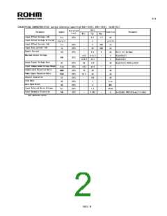
○Block Diagram
○Pin No.・Pin Name
VCC OUT2 -IN2 +IN2
8
7
6
5
-
+
CH2
+
-
CH1
1
2
3
4
OUT1 -IN1 +IN1 VEE
F:SOP8 FV:SSOP-B8 FVM:MSOP8
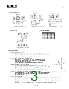
○Application example
(1) Absolute maximum ratings
Absolute maximum ratings are the values which indicate the limits,
within which the given voltage range can be safely charged to the terminal.
However, it does not guarantee the circuit operation.
VCC
(2) The example of disabled circuit application
When there is a circuit not in use, it is recommended to make the
non-inverting input terminal be the potential in the common-mode
input voltage range like in Fig.1.
Circuit operation is guaranteed within Operating Conditions.
-
+
connect
to Vicm
(3) Applied voltage to the input terminal
For normal circuit operation of operational amplifier, please input
voltage for its input terminal within input common mode voltage VCC-2.0[V].
Then, regardless of power supply voltage,VEE+36[V] can be applied to input
terminals without deterioration or destruction of its characteristics.
VEE
(4) Operating power supply (split power supply/single power supply)
The OP-Amp operates if a given level of voltage is applied between VCC and
VEE. Therefore, the OP-Amp can be operated under single power supply or
split power supply.
Fig.1 The example of disabled circuit
(5) Power dissipation(Pd)
If the IC is used under excessive power dissipation. An increase in the chip temperature will cause
deterioration of the radical characteristics of IC.
For example, reduction of current capability. Take consideration of the effective power dissipation and
thermal
design with a sufficient margin. Pd is reference to the provided power dissipation curve.
REV. B

 ROHM [ ROHM ]