2/4
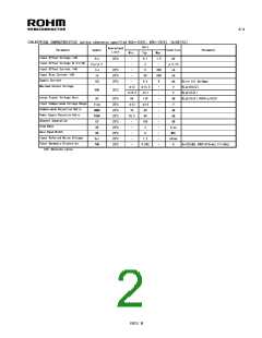
○ELECTRICAL CHARACTERISTICS (unless otherwise specified VCC=+15[V]、VEE=-15[V], Ta=25[℃])
Unit
Guaranteed
Parameter
Symbol
Condition
Parameter
Limit
Min.
Typ.
0.1
2
Max.
1.5
-
Input Offset Voltage (*6)
Input Offset Voltage Drift(*6)
Input Offset Current (*6)
Input Bias Current (*6)
Supply Current
Vio
Vio/ΔT
Iio
25℃
-
mV
μV/℃
nA
-
25℃
25℃
25℃
-
5
200
500
9
Ib
-
50
nA
ICC
-
±12
±10.5
86
5.5
±13.5
±11
110
±14
90
mA
RL=∞ All Op-Amps
Maximum Output Voltage
-
V
RL≧10[kΩ]
VOH
25℃
-
V
RL≧2[kΩ]
Large Signal Voltage Gain
AV
Vicm
CMRR
PSRR
CS
25℃
25℃
25℃
25℃
25℃
25℃
25℃
25℃
25℃
-
dB
RL≧2[kΩ],VOUT=±10[V]
Input Common-mode Voltage Range
Common-mode Rejection Ratio
Power Supply Rejection Ratio
±12
70
-
V
-
dB
76.5
-
90
-
dB
Channel Separation
Slew Rate
105
3
-
dB
SR
-
-
V/us
MHz
uVrms
%
Gain Band Width
GB
-
6
-
Input Referred Noise Voltage
Total Harmonic Distortion
(*6) Absolute value.
Vni
THD
-
1.2
0.002
-
-
-
Av=20[dB],VOUT=5[Vrms],f=1[kHz]
REV. B

 ROHM [ ROHM ]