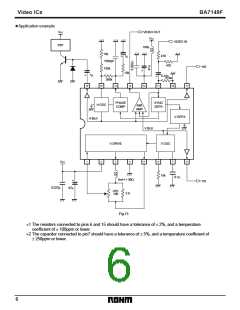
Video ICs
BA7149F
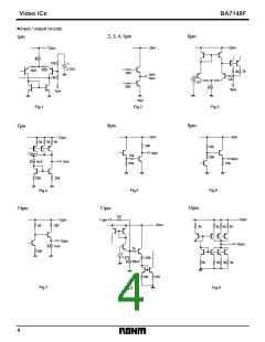
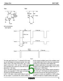
16pin
15pin
2pin
12pin
12pin
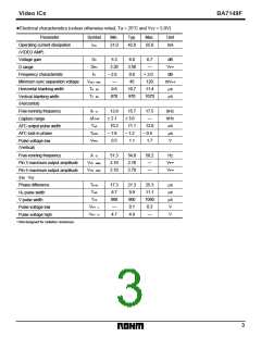
20k
20k
500
16pin
10k 10k
10k
12k
15pin
+
2k 2k
V
2.8V
Fig.11
Fig.10
Circuit operation
Input signals
•
IH
H Pulse only
63.556µ
Pulse IH
0.29V at 11pin
H Pulse only
Pulse IS
adj.at 11pin
4.7µ
262.5H
V Pulse only
16.683m
Pulse IV
Fig.12
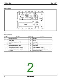
The video signal input to pin 11 is detected by the charg-
ing and discharging of an external capacitor. Sync sepa-
ration is done in the SYNC SEPA block. The H. SYNC
signal is sent to the H. OSC, and the V. SYNC signal is
sync-separated in the vertical sync pulse interval and sup-
plied to the V. OSC block.
cuit, the inherent oscillation period of the oscillation circuit
is made slightly larger than the vertical sync signal period,
so that the sync signal always enters slightly early.
The oscillator output alone is not enough to ensure stable
operation for the vertical deflection output circuit, so it is
amplified by the V. DRIVE block.
The H. OSC block consists of a PLL that oscillates in sync
with the sync-separated H. SYNC signal, and outputs the
HD pulse and horizontal deflection pulse.
The horizontal and vertical blanking signals generated in
the H. OSC and V. OSC blocks are used to erase the hor-
izontal retrace line from the video signal input to pin 11.
The signal is inverted and amplified by a 6dB inverting
amplifier and output as a negative-polarity video signal.
In the V. OSC block, a direct-control method is used with
the sync signal. To synchronize the vertical oscillator cir-
5

 ROHM [ ROHM ]