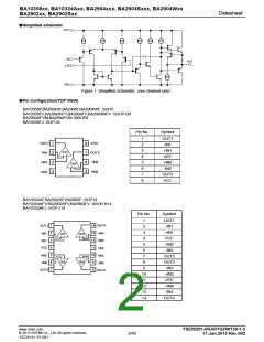
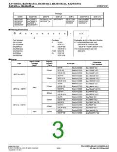
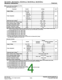
BA10358xx, BA10324Axx, BA2904xxx, BA2904Sxxx, BA2904Wxx
BA2902xx, BA2902Sxx
Datasheet
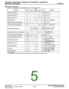
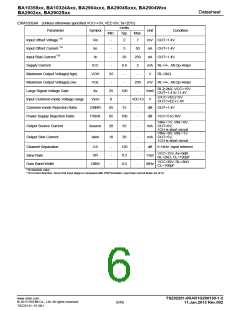
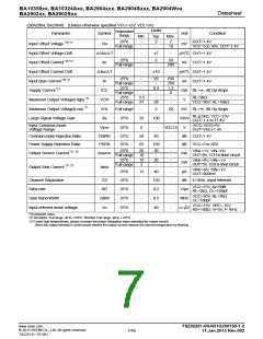
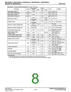
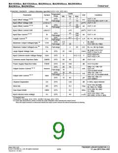
○BA10324A (Unless otherwise specified VCC=+5V, VEE=0V, Ta=25℃)
Limits
Parameter
Symbol
Unit
Condition
Min.
-
Typ.
2
Max.
7
Input Offset Voltage *18
Vio
Iio
mV OUT=1.4V
Input Offset Current *18
-
-
5
20
0.6
-
50
nA OUT=1.4V
Input Bias Current *19
Ib
250
nA OUT=1.4V
Supply Current
ICC
-
2
mA RL=∞,All Op-Amps
Maximum Output Voltage(High)
Maximum Output Voltage(Low)
Large Signal Voltage Gain
Input Common-mode Voltage range
Common-mode Rejection Ratio
Power Supply Rejection Ratio
VOH
VOL
Av
3.5
-
-
V
RL=2kΩ
-
250
mV RL=∞,All Op-Amps
RL≧2kΩ, VCC=15V
V/mV
25
0
100
-
-
OUT=1.4 to 11.4V
(VCC-VEE)=5V
V
Vicm
CMRR
PSRR
VCC-1.5
OUT=VEE+1.4V
65
65
75
100
-
-
dB OUT=1.4V
dB VCC=5 to 30V
VIN+=1V, VIN-=0V
mA OUT=0V,
1CH is short circuit
VIN+=0V, VIN-=1V
mA OUT=5V,
Output Source Current
Output Sink Current
Isource
Isink
20
10
35
20
-
-
1CH is short circuit
Channel Separation
Slew Rate
CS
SR
-
-
-
120
0.2
0.5
-
-
-
dB f=1kHz, input referred
VCC=15V, Av=0dB
V/μs
RL=2kΩ, CL=100pF
VCC=30V, RL=2kΩ
CL=100pF
GBW
MHz
Gain Band Width
*18 Absolute value
*19 Current direction: Since first input stage is composed with PNP transistor, input bias current flows out of IC.
www.rohm.com
© 2013 ROHM Co., Ltd. All rights reserved.
TSZ22111・15・001
TSZ02201-0RAR1G200130-1-2
11.Jan.2013 Rev.002
6/45

 ROHM [ ROHM ]