OP777/OP727/OP747
15V
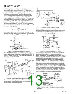
andlimitingdevicepowerdissipationisofprimeimportancein
thesedesigns. Figure7showsanexampleof5V, single-supply
current monitor that can be incorporated into the design of a voltage
regulatorwithfoldbackcurrentlimitingorahighcurrentpower
supplywithcrowbarprotection.Thedesigncapitalizesonthe
OP777’scommon-moderangethatextendstoground.Current
1kꢇ
REF
192
2N2222
1/4 OP747
R2
12kꢇ
3
4
ismonitoredinthepowersupplyreturnwherea0.1
Ω shunt
20kꢇ
+15V
R1
R1
R
resistor, RSENSE, creates a very small voltage drop. The voltage at the
inverting terminal becomes equal to the voltage at the noninverting
terminal through the feedback of Q1, which is a 2N2222 or equiva-
lent NPN transistor. This makes the voltage drop across R1 equal to
the voltage drop across RSENSE. Therefore, the current through Q1
becomes directly proportional to the current through RSENSE, and
the output voltage is given by:
V
O
R(1+ꢈ)
+15V
1/4 OP747
ꢂ15V
R2
R1
ꢆR
R
V
=
V
ꢈ
O
REF
1/4 OP747
ꢈ =
ꢂ15V
Figure 9. Linear Response Bridge
R2
R1
A single-supply current source is shown in Figure 10. Large resistors
are used to maintain micropower operation. Output current can be
adjustedbychangingtheR2Bresistor.Compliancevoltageis:
VOUT = 5V −
× RSENSE × I
L
The voltage drop across R2 increases with IL increasing, so VOUT
decreases with higher supply current being sensed. For the element
values shown, the VOUT is 2.5 V for return current of 1 A.
VL ≤ VSAT − VS
10pF
2.7V TO 30V
5V
100kꢇ
R2 = 2.49kꢇ
100kꢇ
V
OP777
OUT
R1 = 100kꢇ
Q1
R2B
5V
2.7kꢇ
10pF
I
O
R2 = R2A + R2B
R2
R1 ꢉ R2B
= 1mA ꢂ 11mA
+
R2A
97.3kꢇ
OP777
R1 = 100ꢇ
V
R
LOAD
L
I
=
V
S
O
0.1ꢇ
RETURN TO
GROUND
ꢂ
R
SENSE
Figure 10. Single-Supply Current Source
Figure 7. A Low-Side Load Current Monitor
A single-supply instrumentation amplifier using one OP727
amplifierisshowninFigure11.FortruedifferenceR3/R4=
R1/R2. The formula for the CMRR of the circuit at dc is CMRR =
20 × log (100/(1–(R2 × R3)/(R1× R4)). It is common to specify the
accuracy of the resistor network in terms of resistor-to-resistor
percentage mismatch. We can rewrite the CMRR equation to
reflect this CMRR = 20 × log (10000/% Mismatch). The key to
high CMRR is a network of resistors that are well matched from
the perspective of both resistive ratio and relative drift. It should
be noted that the absolute value of the resistors and their absolute
drift are of no consequence. Matching is the key. CMRR is 100 dB
with0.1%mismatchedresistornetwork.TomaximizeCMRR,
one of the resistors such as R4 should be trimmed. Tighter match-
ingof two op amps in one package (OP727) offers a significant
boostinperformanceoverthetripleopampconfiguration.
The OP777/OP727/OP747 is very useful in many bridge applica-
tions. Figure 8 shows a single-supply bridge circuit in which its
output is linearly proportional to the fractional deviation (ꢁ) of
the bridge. Note that ꢁ = ∆R/R.
= 300
15V
AR1ꢉV
REF
V
=
ꢈ + 2.5V
O
2R2
ꢆR1
2
ꢈ =
1/4 OP747
R1
6
RG = 10kꢇ
REF
192
2
10.1kꢇ
1Mꢇ
2.5V
4
3
1Mꢇ
REF
192
0.1ꢀF
15V
15V
4
3
R1(1+ꢈ)
V1
10.1kꢇ
R1
V
O
1/4 OP747
R1(1+ꢈ)
R1
1/4 OP747
R3 = 10.1kꢇ
R2 = 1Mꢇ
R2
2.7V TO 30V
2.7V TO 30V
V2
R4 = 1Mꢇ
R1 = 10.1kꢇ
Figure 8. Linear Response Bridge, Single Supply
V
O
1/2 OP727
In systems where dual supplies are available, the circuit of Figure
9 could be used to detect bridge outputs that are linearly related
to the fractional deviation of the bridge.
V1
V2
1/2 OP727
V
= 100 (V2 ꢂ V1)
O
0.02mV V1 ꢂ V2 290mV
2mV 29V
USE MATCHED RESISTORS
V
OUT
Figure 11. Single-Supply Micropower Instrumentation
Amplifier
–12–
REV. C

 ROCHESTER [ Rochester Electronics ]