OP777/OP727/OP747
Input Over Voltage Protection
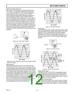
Whentheinputofanamplifierismorethanadiodedropbelow
V
= ꢁ15V
SY
V
IN
V
EE, or above V CC, large currents will flow from the substrate
(V–) or the positive supply (V+), respectively, to the input pins
whichcandestroythedevice.InthecaseofOP777/OP727/
OP747,differentialvoltagesequaltothesupplyvoltagewillnot
causeanyproblem(seeFigure3).OP777/OP727/OP747has
built-in 500 Ω internal current limiting resistors, in series with the
inputs, to minimize the chances of damage. It is a good practice to
keep the current flowing into the inputs below 5 mA. In this con-
text it should also be noted that the high breakdown of the input
transistors removes the necessity for clamp diodes between the
inputs of the amplifier, a feature that is mandatory on many preci-
sion op amps. Unfortunately, such clamp diodes greatly interfere
with many application circuits such as precision rectifiers and
comparators. The OP777/OP727/OP747 series is free from such
limitations.
V
OUT
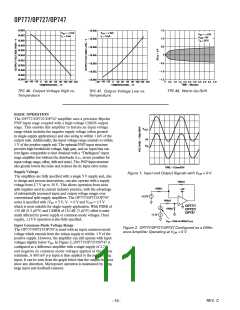
TIME – 400ꢀs/DIV
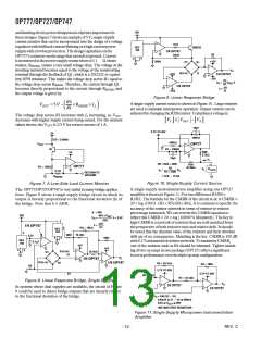
Figure 4. No Phase Reversal
Output Stage
The CMOS output stage has excellent (and fairly symmetric) output
drive and with light loads can actually swing to within 1 mV of both
supplyrails.Thisisconsiderablybetterthansimilaramplifiers
featuring(so-called)rail-to-railbipolaroutputstages.OP777/
OP727/OP747 is stable in the voltage follower configuration and
responds to signals as low as 1 mV above ground in single supply
operation.
30V
OP777/
V p-p = 32V
OP727/
OP747
2.7V TO 30V
Figure 3a. Unity Gain Follower
V
= 1mV
OUT
V
= ꢁ15V
V
= 1mV
SY
IN
OP777/
OP727/
OP747
V
IN
V
OUT
Figure 5. Follower Circuit
TIME – 400ꢀs/DIV
1.0mV
Figure 3b. Input Voltage Can Exceed the Supply Voltage
Without Damage
Phase Reversal
Manyamplifiersmisbehavewhenoneorbothoftheinputsare
forced beyond the input common-mode voltage range. Phase
reversal is typified by the transfer function of the amplifier effectively
reversing its transfer polarity. In some cases this can cause lockup in
servo systems and may cause permanent damage or nonrecoverable
parameter shifts to the amplifier. Many amplifiers feature compensa-
tion circuitry to combat these effects, but some are only effective for
the inverting input. Additionally, many of these schemes only work
for a few hundred millivolts or so beyond the supply rails. OP777/
OP727/OP747hasaprotectioncircuitagainstphasereversal
when one or both inputs are forced beyond their input common-
mode voltage range. It is not recommended that the parts be
continuouslydrivenmorethan3Vbeyondtherails.
TIME – 10ꢀs/DIV
Figure 6. Rail-to-Rail Operation
Output Short Circuit
The output of the OP777/OP727/OP747 series amplifier is protected
from damage against accidental shorts to either supply voltage,
provided that the maximum die temperature is not exceeded on a
long-term basis (see Absolute Maximum Rating section). Current of
up to 30 mA does not cause any damage.
A Low-Side Current Monitor
In the design of power supply control circuits, a great deal of design
effort is focused on ensuring a pass transistor’s long-term reliability
over a wide range of load current conditions. As a result, monitoring
REV. C
–11–

 ROCHESTER [ Rochester Electronics ]