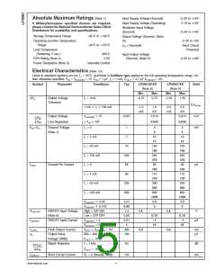
Electrical Characteristics (Note 10) (Continued)
Limits in standard typeface are for TJ = 25˚C, and limits in boldface type applyover the full operating temperature range. Un-
less otherwise specified: VIN = VO(NOM) + 1V, CIN = 1 µF, IL = 1 mA, COUT = 4.7 µF,VON/OFF = 2V.
Symbol
Parameter
Conditions
Typ
LP2981AI-XX
LP2981I-XX
Units
(Note 6)
(Note 6)
Min
Max
Min
Max
(Note 9)
Note 1: Absolute maximum ratings indicate limits beyond which damage to the component may occur. Electrical specifications do not apply when operating the
device outside of its rated operating conditions.
Note 2: The ESD rating of pins 3 and 4 for the SOT-23 package, or pins 5 and 2 for the micro SMD package, is 1 kV.
Note 3: The maximum allowable power dissipation is a function of the maximum junction temperature, T
, the junction-to-ambient thermal resistance, θ , and
JA
J(MAX)
the ambient temperature, T . The maximum allowable power dissipation at any ambient temperature is calculated using:
A
The value of θ for the SOT-23 package is 220˚C/W and the micro SMD package is 225˚C/W. Exceeding the maximum allowable power dissipation will cause
JA
excessive die temperature, and the regulator will go into thermal shutdown.
Note 4: If used in a dual-supply system where the regulator load is returned to a negative supply, the LP2981 output must be diode-clamped to ground.
Note 5: The output PNP structure contains a diode between the V and V
terminals that is normally reverse-biased. Reversing the polarity from V to V
IN OUT
IN
OUT
will turn on this diode (see Application Hints).
Note 6: Limits are 100% production tested at 25˚C. Limits over the operating temperature range are guaranteed through correlation using Statistical Quality Control
(SQC) methods. The limits are used to calculate National’s Average Outgoing Quality Level (AOQL).
Note 7: Dropout voltage is defined as the input to output differential at which the output voltage drops 100 mV below the value measured with a 1V differential.
Note 8: The ON/OFF inputs must be properly driven to prevent misoperation. For details, refer to Application Hints.
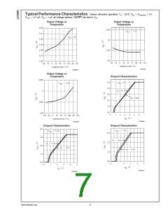
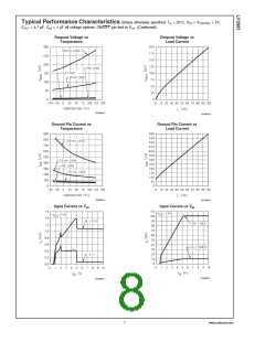
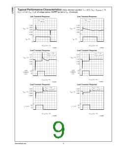
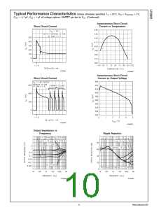
Note 9: See Typical Performance Characteristics curves.
Note 10: Exposing the micro SMD device to direct sunlight will cause misoperation. See Application Hints for additional information.
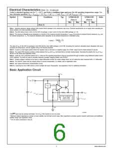
Basic Application Circuit
01250604
*ON/OFF input must be actively terminated. Tie to V if this function is not to be used.
IN
**Minimum Output Capacitance is shown to insure stability over full load current range. More capacitance provides superior dynamic performance and additional
stability margin (see Application Hints).
***Do not make connections to this pin.
5
www.national.com

 ROCHESTER [ Rochester Electronics ]