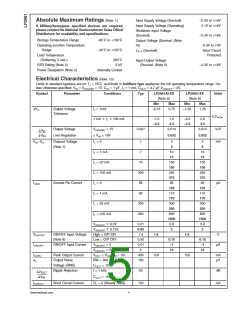
Absolute Maximum Ratings (Note 1)
If Military/Aerospace specified devices are required,
please contact the National Semiconductor Sales Office/
Distributors for availability and specifications.
Input Supply Voltage (Survival)
Input Supply Voltage (Operating)
Shutdown Input Voltage
(Survival)
−0.3V to +16V
2.1V to +16V
−0.3V to +16V
Storage Temperature Range
Operating Junction Temperature
Range
−65˚C to +150˚C
Output Voltage (Survival, (Note
4))
−0.3V to +9V
Short Circuit
Protected
−40˚C to +125˚C
IOUT (Survival)
Lead Temperature
(Soldering, 5 sec.)
260˚C
2 kV
Input-Output Voltage
(Survival, (Note 5)
ESD Rating (Note 2)
Power Dissipation (Note 3)
−0.3V to +16V
Internally Limited
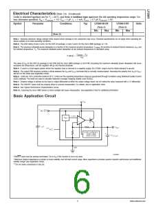
Electrical Characteristics (Note 10)
Limits in standard typeface are for TJ = 25˚C, and limits in boldface type applyover the full operating temperature range. Un-
less otherwise specified: VIN = VO(NOM) + 1V, CIN = 1 µF, IL = 1 mA, COUT = 4.7 µF,VON/OFF = 2V.
Symbol
Parameter
Conditions
Typ
LP2981AI-XX
LP2981I-XX
Units
(Note 6)
(Note 6)
Min
Max
Min
Max
∆VO
Output Voltage
IL = 1mA
−0.75
0.75
−1.25
1.25
Tolerance
%VNOM
%/V
<
<
1 mA IL 100 mA
−1.0
1.0
2.5
−2.0
2.0
3.5
−2.5
−3.5
Output Voltage
Line Regulation
VO(NOM) + 1V
≤ VIN ≤ 16V
IL = 0
0.007
0.014
0.014
0.032
0.032
VIN–VO
Dropout Voltage
(Note 7)
1
3
5
3
5
mV
IL = 1 mA
IL = 25 mA
IL = 100 mA
IL = 0
7
10
10
15
15
70
100
150
250
375
95
100
150
250
375
95
200
65
IGND
Ground Pin Current
µA
125
110
170
300
550
800
1500
0.8
2
125
110
170
300
550
800
1500
0.8
2
IL = 1 mA
IL = 25 mA
IL = 100 mA
80
200
600
<
VON/OFF 0.3V
0.01
0.05
1.4
<
VON/OFF 0.15V
VON/OFF
ION/OFF
ON/OFF Input Voltage
(Note 8)
High = O/P ON
Low = O/P OFF
VON/OFF = 0
1.6
1.6
V
0.50
0.01
5
0.15
−1
0.15
−1
ON/OFF Input Current
µA
VON/OFF = 5V
15
15
IO(PK)
en
Peak Output Current
Output Noise
VOUT ≥ VO(NOM) − 5%
BW = 300 Hz–50 kHz,
COUT = 10 µF
400
160
150
150
mA
µV
Voltage (RMS)
Ripple Rejection
f = 1 kHz
63
dB
COUT = 10 µF
IO(MAX)
Short Circuit Current
RL = 0 (Steady State)
150
mA
www.national.com
4

 ROCHESTER [ Rochester Electronics ]