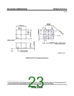
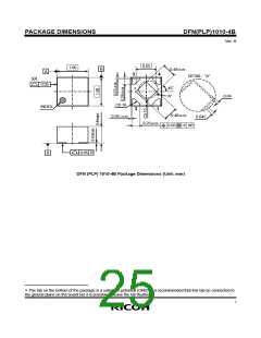
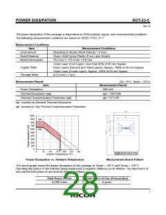
POWER DISSIPATION
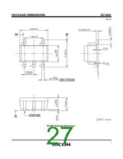
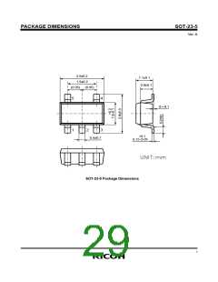
SOT-23-5
Ver. A
The power dissipation of the package is dependent on PCB material, layout, and environmental conditions.
The following measurement conditions are based on JEDEC STD. 51-7.
Measurement Conditions
Item
Measurement Conditions
Mounting on Board (Wind Velocity = 0 m/s)
Environment
Board Material
Board Dimensions
Glass Cloth Epoxy Plastic (Four-Layer Board)
76.2 mm × 114.3 mm × 0.8 mm
Outer Layer (First Layer): Less than 95% of 50 mm Square
Inner Layers (Second and Third Layers): Approx. 100% of 50 mm Square
Outer Layer (Fourth Layer): Approx. 100% of 50 mm Square
φ 0.3 mm × 7 pcs
Copper Ratio
Through-holes
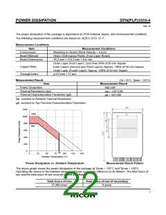
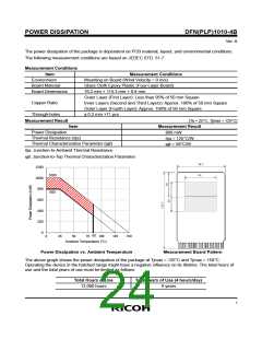
Measurement Result
(Ta = 25°C, Tjmax = 125°C)
Item
Measurement Result
Power Dissipation
660 mW
Thermal Resistance (θja)
θja = 150°C/W
Thermal Characterization Parameter (ψjt)
ψjt = 51°C/W
θja: Junction-to-Ambient Thermal Resistance
ψjt: Junction-to-Top Thermal Characterization Parameter
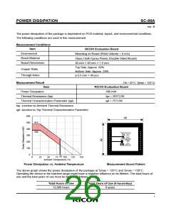
1000
900
800
700
600
500
400
300
200
100
0
830
660
85
0
25
50
75
100 125 150
Ambient Temperature (°C)
Power Dissipation vs. Ambient Temperature
Measurement Board Pattern
The above graph shows the power dissipation of the package at Tjmax = 125°C and Tjmax = 150°C.
Operating the device in the hatched range might have a negative influence on its lifetime. The total hours of
use and the total years of use must be limited as follows:
Total Hours of Use
Total Years of Use (4 hours/day)
13,000 hours
9 years
i

 RICOH [ RICOH ELECTRONICS DEVICES DIVISION ]