Rx5RL
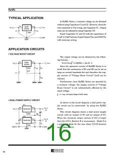
TYPICAL APPLICATION
In Rx5RL Series, a constant voltage can be obtained
without using Capacitors C1 and C2. However, when the
wire connected to Vin is long, use Capacitor C1. Output
noise can be reduced by using Capacitor C2.
VIN
+
VOUT
Rx5RL
VIN
VOUT
SERIES
+
C1
C2
GND
Insert Capacitors C1 and C2 with the capacitance of
0.1µF to 2.0µF between Input/Output Pins and GND Pin
with minimum wiring.
GND
GND
APPLICATION CIRCUITS
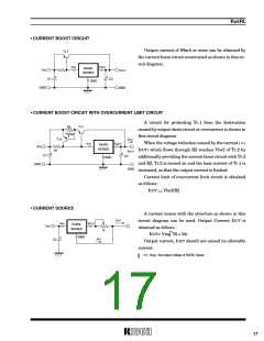
• VOLTAGE BOOST CIRCUIT
The output voltage can be obtained by the follow-
ing formula :
1
VIN
VOUT
Rx5RL
*
VIN
VOUT
VOUT=Vreg · (1+R2/R1) + ISS R · 2
SERIES
Since the quiescent current of Rx5RE Series is so
small that the resistances of R1 and R2 can be set as
large as several hundreds kΩ and therefore the sup-
ply current of “Voltage Boost Circuit” itself can be
reduced.
+
GND
R1
R2
C2
ISS
+
C1
Furthermore, since Rx5RL Series are operated by
a constant voltage, the supply current of “Voltage
Boost Circuit” is not substantially affected by the
input voltage.
1) Vreg : Set Output Voltage of Rx5RL Series.
*
• DUAL POWER SUPPLY CIRCUIT
As shown in the circuit diagram, a dual power sup-
ply circuit can be constructed by using two Rx5RL
Series.
IC1
VIN
VOUT
C1
VOUT1
VIN
Rx5RL20A
5V
+
+
This circuit diagram shows a dual power supply
circuit with an output of 3V and an output of 5V.
When the minimum output current of IC2 is larger
than ISS of IC1, Resistor R is unnecessary. Diode D is
a protection diode for the case where VOUT2 becomes
larger than VOUT1.
D
R
ISS
GND
IC2
VOUT
C3
VIN
+
VOUT2
3V
Rx5RL30A
GND
C2
GND
GND
16

 RICOH [ RICOH ELECTRONICS DEVICES DIVISION ]