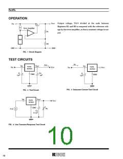
PDF
最近搜索
热门搜索
发布采购

| 型号: | RN5RL25AA-TR-F |
| PDF下载: | 下载PDF文件 查看货源 |
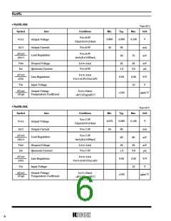
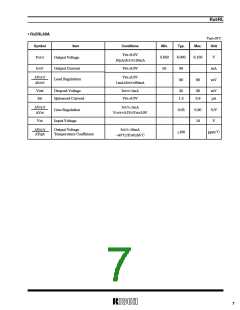
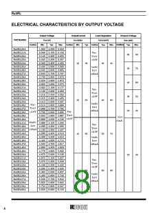
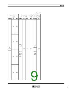
| 内容描述: | [Fixed Positive LDO Regulator, 2.5V, CMOS, PDSO5, ROHS, COMPLIANT, SOT-23, 5 PIN] |
| 分类和应用: | ISM频段光电二极管输出元件调节器 |
| 文件页数/大小: | 18 页 / 609 K |
| 品牌: |  RICOH [ RICOH ELECTRONICS DEVICES DIVISION ] RICOH [ RICOH ELECTRONICS DEVICES DIVISION ] |
专业IC领域供求交易平台:提供全面的IC Datasheet资料和资讯,Datasheet 1000万数据,IC品牌1000多家。